 | –≠–ª–µ–∫—Ç—Ä–æ–Ω–Ω—ã–π –∫–æ–º–ø–æ–Ω–µ–Ω—Ç: ML4812I | –°–∫–∞—á–∞—Ç—å:  PDF PDF  ZIP ZIP |
www.fairchildsemi.com
REV. 1.0.4 5/31/01
Features
∑ Precision buffered 5V reference (±0.5%)
∑ Current-input gain modulator reduces external
components and improves noise immunity
∑ Programmable ramp compensation circuit
∑ 1A peak current totem-pole output drive
∑ Overvoltage comparator helps prevent output voltage
"runaway"
∑ Wide common mode range in current sense comparators
for better noise immunity
∑ Large oscillator amplitude for better noise immunity
Description
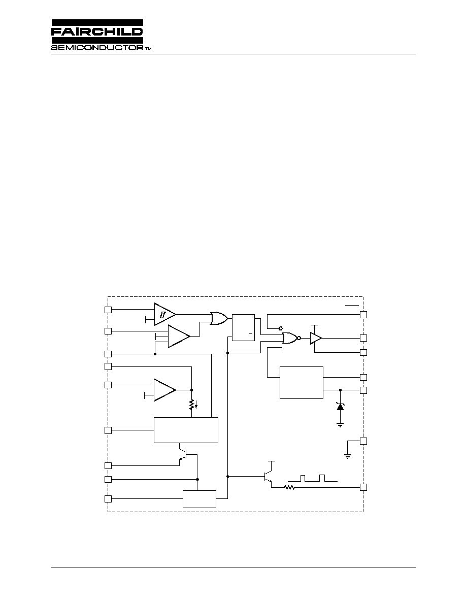
The ML4812 is designed to optimally facilitate a peak
current control boost type power factor correction system.
Special care has been taken in the design of the ML4812 to
increase system noise immunity. The circuit includes a
precision reference, gain modulator, error amplifier, over-
voltage protection, ramp compensation, as well as a high
current output. In addition, start-up is simplified by an under-
voltage lockout circuit with 6V hysteresis.
In a typical application, the ML4812 functions as a current
mode regulator. The current which is necessary to terminate
the cycle is a product of the sinusoidal line voltage times the
output of the error amplifier which is regulating the output
DC voltage. Ramp compensation is programmable with an
external resistor, to provide stable operation when the duty
cycle exceeds 50%.
Block Diagram
(Pin Configuration Shown is for DIP Version)
5V
OVP
ISENSE
GM OUT
EA OUT
ISINE
RAMP COMP
CT
RT
ERROR
AMP
IEA
OSC
1k
UNDER
VOLTAGE
LOCKOUT
SHDN
OUT
PWR GND
VREF
VCC
GND
CLOCK
VCC
EA≠
32V
5
1
2
10
12
11
14
13
15
9
3
4
6
7
16
8
+
≠
5V
+
≠
5V
+
≠
≠
5V
S
R
Q
Q
GAIN MODULATOR
ML4812
Power Factor Controller
ML4812
PRODUCT SPECIFICATION
2
REV. 1.0.4 5/31/01
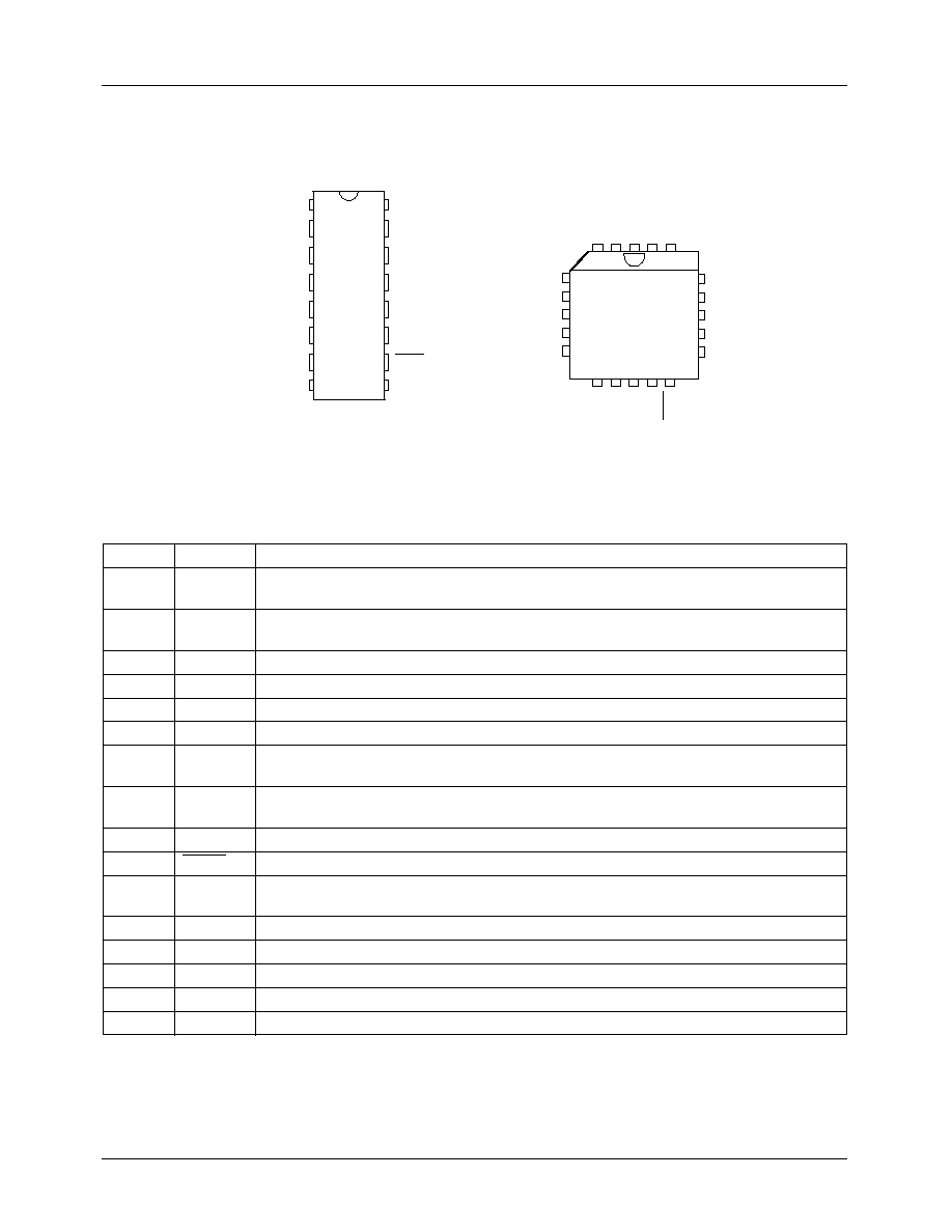
Pin Configuration
Pin Description
Number
Name
Function
1
I
SENSE
Input from the current sense transformer to the non-inverting input of the PWM
comparator.
2
GM OUT
Output of gain modulator. A resistor to ground on this pin converts the current to a
voltage. This pin is clamped to 5V and tied to the inverting input of the PWM comparator.
3
EA OUT
Output of error amplifier.
4
EA≠
Inverting input to error amplifier.
5
OVP
Input to over voltage comparator.
6
I
SINE
Current gain modulator input.
7
RAMP
COMP
Buffered output from the oscillator ramp (C
T
). A resistor to ground sets the current which
is internally subtracted from the product of I
SINE
and I
EA
in the gain modulator.
8
R
T
Oscillator timing resistor pin. A 5V source sets a current in the external resistor which is
mirrored to charge C
T
.
9
CLOCK
Digital clock output.
10 SHDN
A TTL compatible low level on this pin turns off the output.
11
PWR
GND
Return for the high current totem pole output.
12
OUT
High current totem pole output.
13
V
CC
Positive Supply for the IC.
14
V
REF
Buffered output for the 5V voltage reference.
15
GND
Analog signal ground.
16
C
T
Timing capacitor for the oscillator.
1
2
3
4
5
6
7
8
16
15
14
13
12
11
10
9
ISENSE
GM OUT
EA OUT
EA≠
OVP
ISINE
RAMP COMP
RT
CT
GND
VREF
VCC
OUT
PWR GND
SHDN
CLOCK
Top View
ML4812
16-Pin PDIP (P16)
Top View
ML4812
20-Pin PLCC (Q20)
EA OUT
EA≠
NC
OVP
ISINE
VREF
VCC
NC
OUT
PWR GND
GM OUT
I SENSE
NC
C
T
GND
RAMP COMP
R
T
NC
CLOCK
SHDN
4
5
6
7
8
18
17
16
15
14
3
2
1 20 19
9 10 11 12 13
ML4812
PRODUCT SPECIFICATION
3
REV. 1.0.4 5/31/01
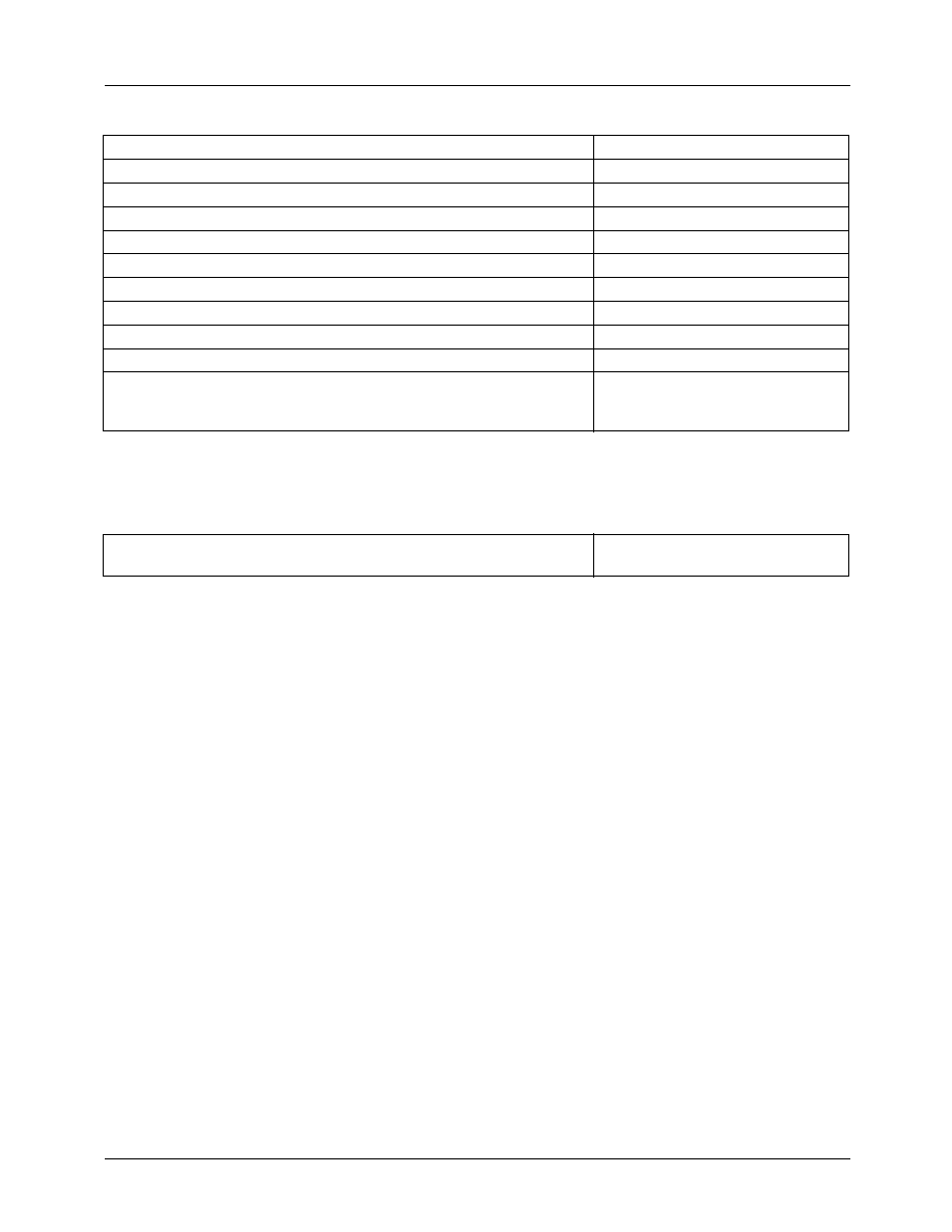
Absolute Maximum Ratings
1
Note:
1. Absolute maximum ratings are those values beyond which the device could be permanently damaged. Absolute maximum
ratings are stress ratings only and functional device operation is not implied.
Operating Conditions
Supply Current (I
CC
) 30mA
Output Current Source or Sink (OUT) DC
1.0A
Output Energy (capacitive load per cycle)
5µJ
Gain Modulator I
SINE
Input (I
SINE
)
1.2mA
Error Amp Sink Current (EA OUT)
10mA
Oscillator Charge Current
2mA
Analog Inputs (I
SENSE
, EA≠, OVP)
≠0.3V to 5.5V
Junction Temperature
150∞C
Storage Temperature Range
≠65∞C to 150∞C
Lead Temperature (soldering 10 sec.)
260∞C
Thermal Resistance (
JA
)
20-Pin PLCC
16-Pin PDIP
60∞C/W
65∞C/W
Temperature Range
ML4812CX
0∞C to 70∞C
PRODUCT SPECIFICATION
ML4812
REV. 1.0.4 5/31/01
4
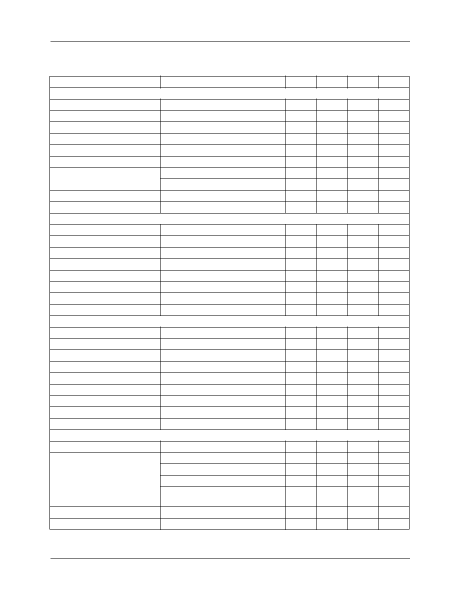
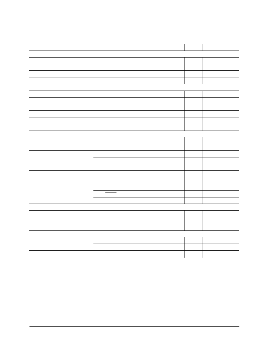
Electrical Characteristics
Unless otherwise specified, V
CC
= 15V , R
T
= 14k
, C
T
= 1000pF, T
A
= Operating Temperature Range (Notes 1, 2).
Parameter
Conditions
Min.
Typ.
Max.
Units
Oscillator
Initial Accuracy
T
J
= 25∞C
91
98
105
kHz
Voltage Stability
12V < V
CC
< 18V
0.3
%
Temperature Stability
2
%
Total Variation
Line, temperature
90
108
kHz
Ramp Valley to Peak
3.3
V
R
T
Voltage
4.8
5.0
5.2
V
Discharge Current (R
T
open)
T
J
= 25∞C, V
CT
= 2V
7.8
8.4
9.0
mA
V
CT
= 2V
7.3
8.4
9.3
mA
Clock Out Voltage Low
RL = 16k
0.2
0.5
V
Clock Out Voltage High
RL = 16k
3.0
3.5
V
Reference
Output Voltage
T
J
= 25∞C, I
O
= 1mA
4.95
5.00
5.05
V
Line Regulation
12V < V
CC
< 25V
2
20
mV
Load Regulation
1mA < IO < 20mA
2
20
mV
Temperature Stability
0.4
%
Total Variation
Line, load, temp.
4.9
5.1
V
Output Noise Voltage
10Hz to 10kHz
50
µV
Long Term Stability
T
J
= 125∞C, 1000 hours
5
25
mV
Short Circuit Current
V
REF
= 0V
≠30
≠85
≠180
mA
Error Amplifier
Input Offset Voltage
±15
mV
Input Bias Current
≠0.1
≠1.0
µA
Open Loop Gain
1 < V
EA OUT
< 5V
60
75
dB
PSRR
12V < V
CC
< 25V
60
75
dB
Output Sink Current
V
EA OUT
= 1.1V, V
EA≠
= 6.2V
2
12
mA
Output Source Current
V
EA OUT
= 5.0V, V
EA
≠ = 4.8V
≠0.5
≠1.0
mA
Output High Voltage
I
EA OUT
= ≠0.5mA, V
EA
≠ = 4.8V
5.3
5.5
V
Output Low Voltage
I
EA OUT
= 1mA, V
EA
≠ = 6.2V
0.5
1.0
V
Unity Gain Bandwidth
1.0
MHz
Gain Modulator
I
SINE
Input Voltage
I
SINE
= 500µA
0.4
0.7
0.9
V
Output Current (GM OUT)
I
SINE
= 500µA, EA≠ = V
REF
≠ 20mV
430
470
510
µA
I
SINE
= 500µA, EA≠ = V
REF
+ 20mV
3
10
µA
I
SINE
= 1mA, EA≠ = V
REF
≠ 20mV
860
940
1020
µA
I
SINE
= 500µA, EA≠ = V
REF
≠ 20mV,
I
RAMP COMP
= 50µA
455
µA
Bandwidth
200
kHz
PSRR
12V < V
CC
< 25V
70
dB
ML4812
PRODUCT SPECIFICATION
5
REV. 1.0.4 5/31/01
Notes:
1. Limits are guaranteed by 100% testing, sampling, or correlation with worst-case test conditions.
2. V
CC
is raised above the Startup Threshold first to activate the IC, then returned to 15V.
OVP Comparator
Input Offset Voltage
Output Off
≠25
+5
mV
Hysteresis
Output On
95
105
115
mV
Input Bias Current
≠0.3
≠3
µA
Propagation Delay
150
ns
PWM Comparator: I
SENSE
Input Offset Voltage
±15
mV
Input Offset Current
±1
µA
Input Common Mode Range
≠0.2
5.5
V
Input Bias Current
≠2
≠10
µA
Propagation Delay
150
ns
I
LIMIT
Trip Point
V
GM OUT
= 5.5V
4.8
5
5.2
V
Output
Output Voltage Low
I
OUT
= ≠20mA
0.1
0.4
V
I
OUT
= ≠200mA
1.6
2.2
V
Output Voltage High
I
OUT
= 20mA
13
13.5
V
I
OUT
= 200mA
12
13.4
V
Output Voltage Low in UVLO
I
OUT
= ≠5mA, V
CC
= 8V
0.1
0.8
V
Output Rise/Fall Time
C
L
= 1000pF
50
ns
Shutdown
V
IH
2.0
V
V
IL
0.8
V
I
IL
, V
SHDN
= 0V
≠1.5
mA
IIH, V
SHDN
= 5V
10
µA
Under-Voltage Lockout
Startup Threshold
15
16
17
V
Shutdown Threshold
9
10
11
V
V
REF
Good Threshold
4.4
V
Supply
Supply Current
Start-Up, V
CC
= 14V, T
J
= 25∞C
0.8
1.2
mA
Operating, T
J
= 25∞C
20
25
mA
Internal Shunt Zener Voltage
I
CC
= 30mA
25
30
34
V
Electrical Characteristics
(Continued)
Unless otherwise specified, V
CC
= 15V , R
T
= 14k
, C
T
= 1000pF, T
A
= Operating Temperature Range (Notes 1, 2).
Parameter
Conditions
Min.
Typ.
Max.
Units