 | ÐлекÑÑоннÑй компоненÑ: ML4819CS | СкаÑаÑÑ:  PDF PDF  ZIP ZIP |
Äîêóìåíòàöèÿ è îïèñàíèÿ www.docs.chipfind.ru
+
R
T
I
SENSE
B
I
SENSE
A
INV A
OVP
EA OUT A
I
SINE
RAMP COMP
C
T
ERROR
AMP
+
5V
I
EA
I
MULT
OSC
SLOPE
COMPENSATION
UNDER
VOLTAGE
LOCKOUT
S
R
Q
S
R
Q
DUTY CYCLE
I
LIM
PWM B
OUT B
PGND B
PGND A
V
REF
V
CC
V
CC
V
CC
GND
OUT A
GM OUT
5V
5V
0.7V
1V
10
20
12
7
11
9
8
14
18
17
16
15
13
1
3
2
5
4
6
19
GAIN MODULATOR
PWM
CONTROLLER
POWER FACTOR
CONTROLLER
+
+
+
+
Please See Ml4824 for New Designs
May 1997
ML4819
Power Factor and PWM Controller "Combo"
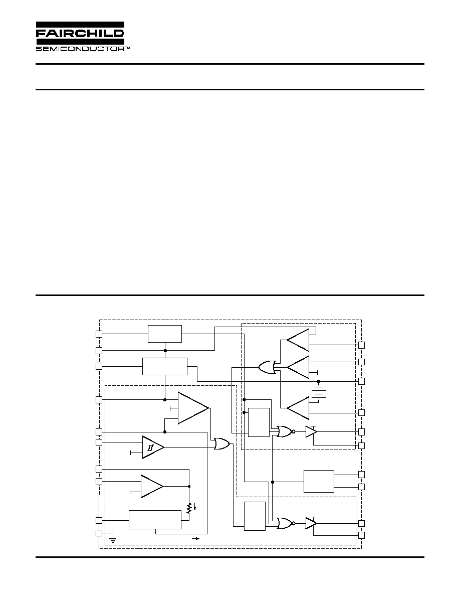
GENERAL DESCRIPTION
The ML4819 is a complete boost mode Power factor
Controller (PFC) which also contains a PWM controller.
The PFC circuit is similar to the ML4812 while the PWM
controller can be used for current or voltage mode control
for a second stage converter. Since the PWM and PFC
circuits share the same oscillator, synchronization of the
two stages is inherent. The outputs of the controller IC
provide high current (>1A peak) and high slew rate to
quickly charge and discharge MOSFET gates. Special care
has been taken in the design of the ML4819 to increase
system noise immunity.
The PFC section is of the peak current sensing boost type,
using a current sense transformer or current sensing
MOSFETs to non-dissipatively sense switch current. This
gives the system overall efficiency over average current
sensing control method.
The PWM section includes cycle by cycle current limiting,
precise duty cycle limiting for single ended converters,
and slope compensation.
BLOCK DIAGRAM
FEATURES
s
Two 1A peak current totem-pole output drivers
s
Precision buffered 5V reference (
±
1%)
s
Large oscillator amplitude for better noise immunity
s
Precision duty cycle limit for PWM section
s
Current input gain modulator improves noise immunity
s
Programmable Ramp Compensation circuit
s
Over-Voltage comparator helps prevent output
"runaway"
s
Wide common mode range in current sense
compensators for better noise immunity
s
Under-Voltage Lockout circuit with 6V hysteresis
REV. 1.0 10/10/2000
ML4819
2
REV. 1.0 10/10/2000
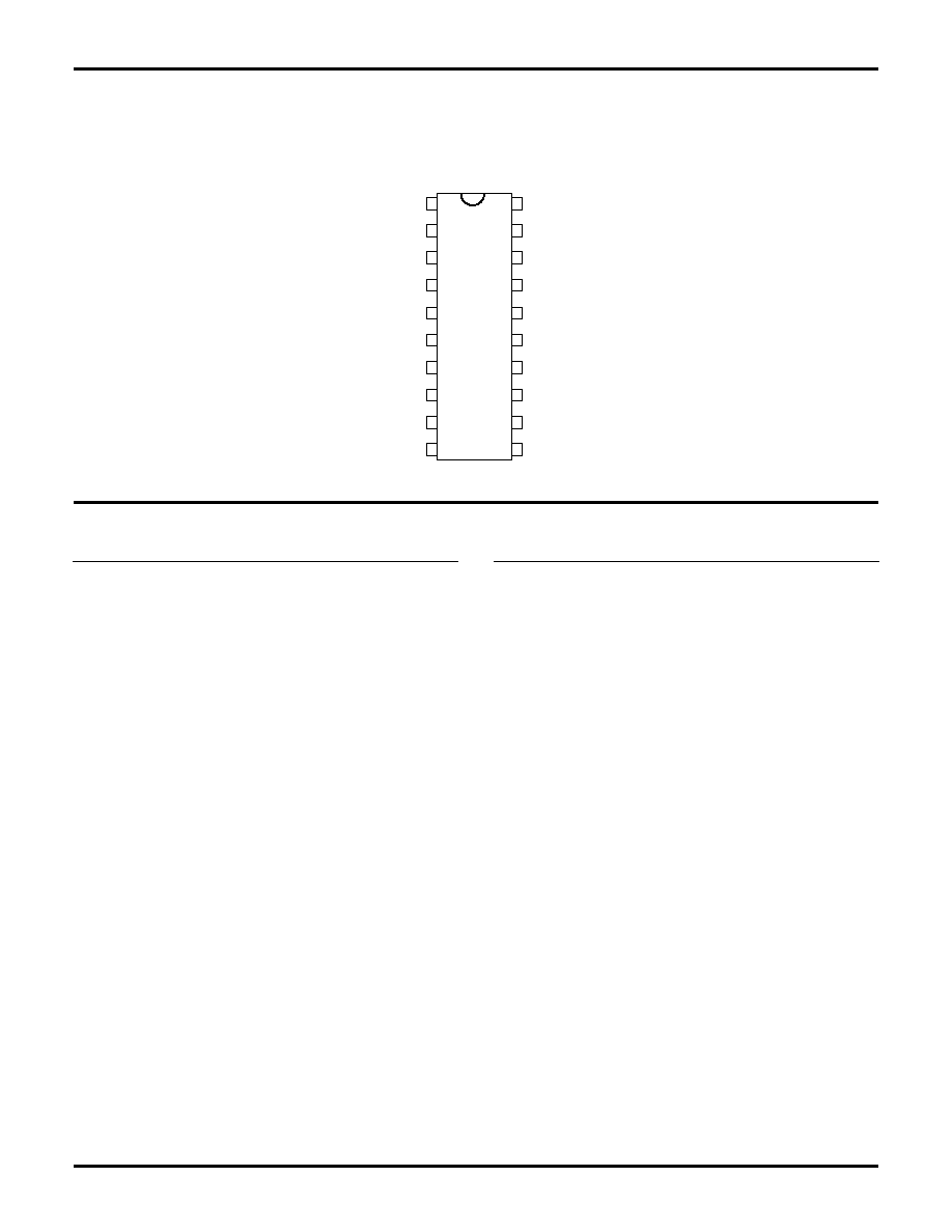
PIN CONFIGURATION
PIN
NAME
FUNCTION
PIN
NAME
FUNCTION
1
I
SENSE
A
Input form the PFC current sense
transformer to the PWM comparator
(+). Current Limit occurs when this
point reaches 5V.
2
OVP
Input to Over-Voltage comparator.
3
GM OUT
Output of Gain Modulator. A resistor
to ground on this pin converts the
current to a voltage.
4
EA OUT A
Output of error amplifier.
5
INV A
Inverting input to error amplifier.
6
I
SINE
Current Multiplier input.
7
DUTY CYCLE PWM controller duty cycle is limited
by setting this pin to a fixed voltage.
8
PWM B
Error voltage feedback input.
9
I
SENSE
B
Input for Current Sense resistor for
current mode operation or for
Oscillator ramp for voltage mode
operation.
10 R
T
Oscillator timing resistor pin. A 5V
source across this resistor sets the
charging current for C
T
11 I
LIM
Cycle by cycle PWM current limit.
Exceeding 1V threshold on this pin
terminates the PWM cycle.
12 RAMP COMP Buffered output from the Oscillator
Ramp (C
T
). A resistor to ground sets a
current, 1/2 of which is sourced on
pins 9 and 11.
13 GND B
Return for the high current totem pole
output of the PWM controller.
14 OUT B
PWM controller totem pole output.
15 V
CC
Positive Supply for the IC.
16 OUT A
PFC controller totem pole output.
17 GND A
Return for the high current totem pole
output of the PFC controller.
18 V
REF
Buffered output for the 5V voltage
reference
19 GND
Analog signal ground.
20 C
T
Timing Capacitor for the Oscillator.
PIN DESCRIPTION
ML4819
20-Pin PDIP
I
SENSE
A
OVP
GM OUT
EA OUT A
INV A
I
SINE
DUTY CYCLE
PWM B
I
SENSE
B
R
T
C
T
GND
V
REF
PGND A
OUT A
V
CC
OUT B
PGND B
RAMP COMP
I
LIM
1
2
3
4
5
6
7
8
9
10
20
19
18
17
16
15
14
13
12
11
TOP VIEW
ML4819
REV. 1.0 10/10/2000
3
ELECTRICAL CHARACTERISTICS
Unless otherwise specified, R
T
= 14k
, C
T
= 1000pF, T
A
= Operating Temperature Range, V
CC
= 15V (Notes 1, 2).
PARAMETER
CONDITIONS
MIN
TYP
MAX
UNITS
OSCILLATOR
Initial Accuracy
T
J
= 25
°
C
90
97
104
kHz
Voltage Stability
12V < V
CC
< 18V
0.2
%
Temperature Stability
2
%
Total Variation
Line, temp.
88
106
kHz
Ramp Valley
0.9
V
Ramp Peak
4.3
V
R
T
Voltage
4.8
5.0
5.2
V
Discharge Current (PWM B open)
T
J
= 25
°
C, V
OUT A
= 2V
7.5
8.4
9.3
mA
V
OUT A
= 2V
7.2
8.4
9.5
mA
DUTY CYCLE LIMIT COMPARATOR
Input Offset Voltage
15
15
mV
Input Bias Current
2
10
µ
A
Duty Cycle
V
DUTY CYCLE
= V
REF/2
43
45
49
%
REFERENCE
Output Voltage
T
J
= 25
°
C, I
O
= 1mA
4.95
5.00
5.05
V
Line Regulation
12V < V
CC
< 25V
2
20
mV
Load Regulation
1mA < I
O
< 20mA
8
25
mV
Temperature Stability
0.4
%
Total Variation
Line, load, temperature
4.9
5.1
V
Output Noise Voltage
10Hz to 10kHz
50
µ
V
Long Term Stability
T
J
= 125
°
C, 1000 hours, (Note 1)
5
25
mV
Short Circuit Current
V
REF
= 0V
30
85
180
mA
ERROR AMPLIFIER
Input Offset Voltage
15
15
mV
Input Bias Current
0.1
1.0
µ
A
Open Loop Gain
1 < V
EA OUT A
< 5V
60
75
dB
PSRR
12V < V
CC
< 25V
60
90
dB
Output Sink Current
V
EA OUT A
= 1.1V, V
INV A
= 5.2V
2
12
mA
Output Source Current
V
EA OUT A
= 5.0V, V
INV A
= 4.8V
0.5
1.0
mA
ABSOLUTE MAXIMUM RATINGS
Absolute maximum ratings are those values beyond which
the device could be permanently damaged. Absolute
maximum ratings are stress ratings only and functional
device operation is not implied.
Supply Voltage (V
CC
) ................................................. 35V
Output Current, Source or Sink (RAMP COMP)
DC ....................................................................... 1.0A
Output Energy (capacitive load per cycle) ................... 5
µ
J
Multiplier I
SINE
Input (I
SINE
) ................................... 1.2mA
Error Amp Sink Current (GM OUT) ........................ 10mA
Oscillator Charge Current ........................................ 2mA
Analog Inputs (ISENSE A, EA OUT A, INV A)
............................................................... 0.3V to 5.5V
Junction Temperature ............................................. 150
°
C
Storage Temperature Range ..................... 65
°
C to 150
°
C
Lead Temperature (soldering 10 sec.) ..................... 260
°
C
Thermal Resistance (
JA
)
Plastic DIP or SOIC ......................................... 60
°
C/W
OPERATING CONDITIONS
Temperature Range
ML4819C .................................................. 0
°
C to 70
°
C
ML4819
4
REV. 1.0 10/10/2000
ELECTRICAL CHARACTERISTICS
(Continued)
PARAMETER
CONDITIONS
MIN
TYP
MAX
UNITS
ERROR AMPLIFIER (continued)
Output High voltage
I
EA OUT A
= 0.5mA, V
INV A
= 4.8V
6.5
7.0
V
Output Low Voltage
I
EA OUT A
= 2mA, V
INV A
= 5.2V
0.7
1.0
V
Unity Gain Bandwidth
1.0
MHz
GAIN MODULATOR
I
SINE
Input Voltage
I
SINE
= 500
µ
A
0.4
0.7
0.9
V
Output Current (GM OUT)
I
SINE
= 500
µ
A, INV A = V
REF
20mV
460
495
505
µ
A
I
SINE
= 500
µ
A, INV A = V
REF
+ 20mV
0
10
µ
A
I
SINE
= 1mA, INV A = V
REF
20mV
900
990
1005
µ
A
Bandwidth
200
kHz
PSRR
12V < V
CC
< 25V
70
dB
SLOPE COMPENSATION CIRCUIT
RAMP COMP Voltage
V
C(T)
1
V
I
OUT
(I
SENSE
A or I
SENSE
B)
I
RAMP COMP
= 100
µ
A (Note 3)
45
48
51
µ
A
OVP COMPARATOR
Input Offset Voltage
Output Off
15
15
mV
Hysteresis
Output On
100
120
140
mV
Input Bias Current
0.3
3
µ
A
Propagation Delay
150
ns
I
SENSE
COMPARATORS
Input Common Mode Range
0.2
5.5
V
Input Offset Voltage
I
SENSE
A
15
15
mV
I
SENSE
B
0.4
0.7
0.9
V
Input Bias Current
3
10
µ
A
Input Offset Current
3
0
3
µ
A
Propagation Delay
150
ns
I
LIMIT
(A) Trip Point
V
OVP
= 5.5V
4.8
5
5.2
V
I
LIM
COMPARATOR
I
LIMIT
Trip Point
.95
1.0
1.05
V
Input Bias Current
2
10
µ
A
Propagation Delay
150
ns
OUTPUT DRIVERS
Output Voltage Low
I
OUT
= 20mA
0.1
0.4
V
I
OUT
= 200mA
1.6
2.2
V
Output Voltage High
I
OUT
= 20mA
13
13.5
V
I
OUT
= 200mA
12
13.4
V
Output Voltage Low in UVLO
I
OUT
= 1mA, V
CC
= 8V
0.1
0.8
V
Output Rise/Fall Time
C
L
= 1000pF
50
ns
ML4819
REV. 1.0 10/10/2000
5
FUNCTIONAL DESCRIPTION
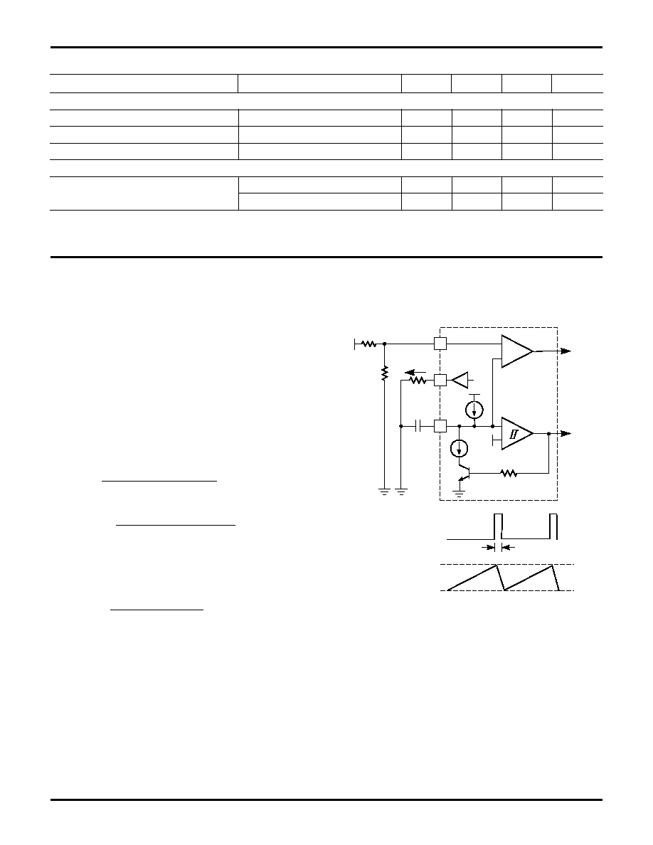
OSCILLATOR
The ML4819 oscillator charges the external capacitor (C
T
)
with a current (I
SET
) equal to 5/R
SET
. When the capacitor
voltage reaches the upper threshold, the comparator
changes state and the capacitor discharges to the lower
threshold through Q1. While the capacitor is discharging,
the clock provides a high pulse.
The oscillator period can be described by the following
relationship:
t
OSC
= t
RAMP
+ t
DEADTIME
where:
t
=
C(Ramp Valley to Peak)
I
RAMP
SET
and:
t
C(Ramp Valley to Peak)
8.4mA - I
DEADTIME
SET
=
The maximum duty cycle of the PWM section can be
limited by setting a threshold on pin 7. when the C
T
ramp
is above the threshold at pin 7, the PWM output is held
off and the PWM flip-flop is set:
D
D
(V
- 0.9)
3.4
LIMIT
OSC
PIN7
×
where:
D
LIMIT
= Desired duty cycle limit
D
OSC
= Oscillator duty cycle
ELECTRICAL CHARACTERISTICS
(Continued)
PARAMETER
CONDITIONS
MIN
TYP
MAX
UNITS
UNDER-VOLTAGE LOCKOUT
Start-Up Threshold
15
16
17
V
Shut-Down Threshold
9
10
11
V
V
REF
Good Threshold
4.4
V
SUPPLY
Supply Current
Start-Up, V
CC
= 14V
0.6
1.2
mA
Operating, T
J
= 25
°
C
25
35
mA
Note 1: Limits are guaranteed by 100% testing, sampling, or correlation with worst-case test conditions.
Note 2: V
CC
is raised above the Start-Up Threshold first to activate the IC, then returned to 15V.
Note 3: PWM comparator bias currents are subtracted from this reading.
Figure 1. Oscillator Block Diagram
R
T
I
SET
C
T
CLOCK
DUTY CYCLE
20
10
I
SET
V
REF
5V
+5V
TO PWM
LATCH B
TO PWM
LATCHES
8.4mA
Q1
CLOCK
t
D
RAMP PEAK
RAMP VALLEY
C
T
7
+
+