 | ÐлекÑÑоннÑй компоненÑ: ML4821 | СкаÑаÑÑ:  PDF PDF  ZIP ZIP |
Äîêóìåíòàöèÿ è îïèñàíèÿ www.docs.chipfind.ru
www.fairchildsemi.com
REV. 1.0.2 6/19/01
Features
· Average current sensing for lowest possible harmonic
distortion
· Average line compensation with brown-out control
· Precision buffered 5V reference
· 1A peak current totem-pole output drive
· Overvoltage comparator eliminates output "runaway" due
to load removal
· Wide common mode range in current sense comparators
for better noise immunity
· Large oscillator amplitude for better noise immunity
· Output driver internally limited to 17V
· "Sleep mode" shutdown input
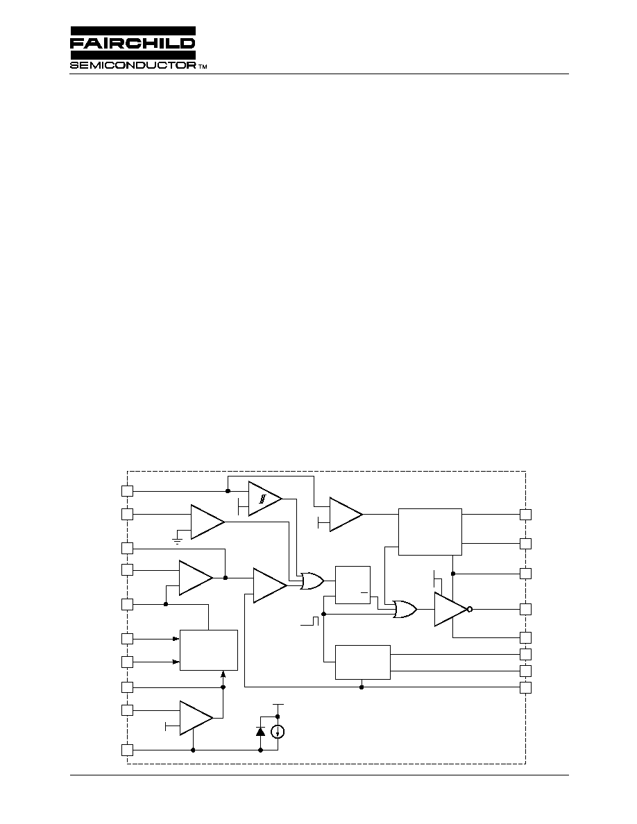
General Description
The ML4821 provides complete control for a "boost" type
power factor correction system using the average current
sensing method. Special care has been taken in the design of
the ML4821 to increase system noise immunity. The circuit
includes a precision reference, gain modulator, average
current error amplifier, output error amplifier, over-voltage
protection comparator, shutdown logic, as well as a high
current output. In addition, start-up is simplified by an under-
voltage lockout circuit.
In a typical application, the ML4821 controls the AC input
current by adjusting the pulse width of the output MOSFET.
This modulates the line current so that its shape conforms to
the shape of the input voltage. The reference for the current
regulator is a product of the sinusoidal line voltage times the
output of the error amplifier which is regulating the output
DC voltage. Average line voltage compensation is provided
in the gain modulator to ensure constant loop gain over a
wide input voltage range. This compensation includes a
special "brown-out" control which reduces output power
below 90V RMS input.
Block Diagram
11
1
2
3
4
5
8
6
7
9
16
18
15
14
13
12
10
17
+
+
+
+
+
+
V
REF
SOFT START
V
REF
EA
EA OUT
V
RMS
I
SINE
OUT
GAIN
MODULATOR
IA
IA+
IA OUT
I
LIM
OVP
V
REF
0.7V
R
S
Q
UNDER
VOLTAGE
LOCKOUT
OSC
V
REF
V
LIMIT
17V
GND
V
CC
OUT
PGND
R
T
SYNC
C
T
SLEEP
ML4821
Power Factor Controller
ML4821
PRODUCT SPECIFICATION
2
REV. 1.0.2 6/19/01
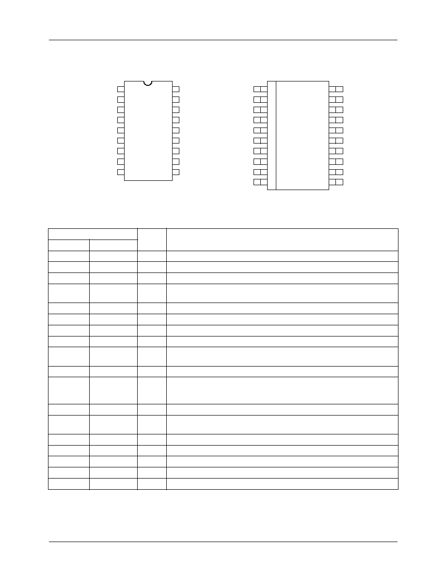
Pin Connection
Pin Description
Pin Number
Name
Function
18-Pin DIP
20-Pin SOIC
1
1
I
LIM
Peak cycle-by-cycle current limit input
2
2
IA OUT
Output and compensation node of the average current error amplifier
3
3
IA
Inverting input of the average current error amplifier
4
4
IA+
Non-Inverting input of the average current error amplifier and output of the
gain modulator
5
5
I
SINE
Gain modulator input
6
6
EA OUT Output of output voltage error amplifier
7
7
INV
Inverting input to error amplifier
8
8
V
RMS
Input for average line voltage compensation
9
9
SOFT
START
Normally connected to soft start capacitor
10
12
SYNC
Oscillator synchronization input
11
13
OVP
Inhibits output pulses when the voltage at this pin exceeds 5V. Also,
when the voltage at this pin is less than 0.7V, the IC goes into low current
shut-down mode.
12
14
R
T
Timing resistor for the oscillator
13
15
PWR
GND
Return for the high current totem pole output
14
16
OUT
High current totem pole output
15
17
V
CC
Positive supply for the IC
16
18
V
REF
Buffered output for the 5V voltage reference
17
19
C
T
Timing capacitor for the oscillator.
18
20
GND
Analog signal ground
I
LIM
IA OUT
IA
IA+
I
SINE
EA OUT
EA
V
RMS
SOFT START
GND
C
T
V
REF
V
CC
OUT
PGND
R
T
OVP
SYNC
I
LIM
IA OUT
IA
IA+
I
SINE
EA OUT
EA
V
RMS
SOFT START
N/C
GND
C
T
V
REF
V
CC
OUT
PGND
R
T
OVP
SYNC
N/C
1
2
3
4
5
6
7
8
9
10
20
19
18
17
16
15
14
13
12
11
1
2
3
4
5
6
7
8
9
18
17
16
15
14
13
12
11
10
TOP VIEW
18-Pin PDIP (P18)
20-Pin SOIC (S20)
TOP VIEW
PRODUCT SPECIFICATION
ML4821
REV. 1.0.2 6/19/01
3
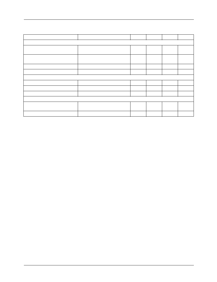
Absolute maximum ratings
Absolute maximum ratings are those values beyond which the device could be permanently damaged. Absolute maximum
ratings are stress ratings only and functional device operation is not implied.
Operating Conditions
Parameter
Min
Max
Units
Supply Current (I
CC
)
35
mA
OUT Current, Source or Sink
1.0
A
Output Energy (capacitive load per cycle)
5
µJ
I
SINE
Input Current
1.2
mA
EA OUT Source Current
50
mA
Oscillator Charge Current
2
mA
Input Voltage
GND 0.3V
5.5
V
Junction Temperature
150
°C
Storage Temperature Range
65
150
°C
Lead Temperature (Soldering 10 sec.)
260
°C
Thermal Resistance (
JA
)
Plastic DIP
Plastic SOIC
75
95
°C/W
°C/W
Temperature Range
Min
Max
Units
ML4821CX
0
70
°C
Electrical Characteristics
Unless otherwise specified, R
T
= 6.2k
, C
T
= 720pF, T
A
= Operating Temperature Range, V
CC
= 15V (Notes 1 & 2).
Parameter
Conditions
Min.
Typ.
Max.
Units
Oscillator
Initial accuracy
T
A
= 25°C
90
100
110
kHz
Voltage stability
12V < V
CC
< 18V
1
%
Temperature stability
2
%
Total Variation
Line, Temperature
85
115
kHz
Ramp Valley to Peak
4.7
5.2
5.6
V
R
T
Voltage
4.8
5.0
5.2
V
Discharge Current
C
T
= 2V, R
T
= Open
7.8
8.4
9.3
mA
SYNC Input Threshold
1.5
2.0
3.0
V
Reference
Output Voltage
T
A
= 25°C, I
O
= 1mA
4.95
5.00
5.05
V
Line regulation
12V < V
CC
< 24V
2
10
mV
Load regulation
1mA < I
O
< 20mA
2
15
mV
Temperature stability
.4
%
Total Variation
line, load, temp
4.9
5.1
V
Output Noise Voltage
10Hz to 10kHz
50
µV
Long Term Stability
T
A
= 125°C, 1000 hrs
5
25
mV
Short Circuit Current
V
REF
= 0V
30
85
180
mA
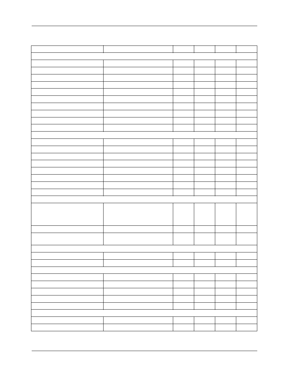
ML4821
PRODUCT SPECIFICATION
4
REV. 1.0.2 6/19/01
Voltage Error Amplifier
Input Offset Voltage
0
15
mV
Input Bias Current
50
800
nA
Open Loop Gain
2 < EA OUT < 6V
60
75
dB
PSRR
12V < V
CC
< 24V
70
100
dB
Output Sink Current
EA OUT = 4V, INV = 5.5V
300
500
µA
Output Source Current
EA OUT
= 4.0V, INV
= 4.8V
10
30
mA
Output High Voltage
I
PIN6
= 5mA, V
PIN7
= 4.8V
7.0
7.5
V
Output Low Voltage
I
PIN6
= 0, EA = 5.5V
0
0.5
V
Unity Gain Bandwidth
1.0
MHz
Soft Start Charge Current
V
PIN9
= 4V
22
38
50
µA
Current Error Amplifier
Input Offset Voltage
5
0
5
mV
Input Bias Current
0.15
1
µA
Input Offset Current
400
nA
Open Loop Gain
2 < EA OUT < 7V
80
100
dB
PSRR
12V < V
CC
< 24V
65
85
dB
Output Voltage Low
I
OL
= 300µA
0
0.5
V
Output Voltage High
I
OH
= 10mA
7.0
7.5
V
Input Common Mode Range
0.3
2.5
V
Gain Modulator
Gain
V
INV
= 4.8V, V
RMS
= 0V
V
INV
= 4.8V, V
RMS
= 1.75V
V
INV
= 4.8V, V
RMS
= 2.6V
V
INV
= 4.8V, V
RMS
= 5.2V
0.75
3.1
1.25
0.22
1.2
3.88
1.75
0.38
1.3
4.5
2.15
0.50
Output Current
V
INV
= 5.2V, V
RMS
= 5.2V
2
4
µA
Output Current Limit
V
INV
= 4.8V, I
SINE
= 500
µ
A,
V
RMS
= 1.75V
360
395
420
µA
I
LIM
Comparator
Input Offset Voltage
+15
mV
Input Bias Current
100
200
µA
OVP Comparator
Input Offset Voltage
Output Off
25
5
mV
Hysteresis
Output On
85
105
130
mV
Input Bias Current
0.3
3
µA
Propagation Delay
150
ns
Shutdown Threshold
0.4
0.7
1.0
V
PWM Comparator
Input Common Mode Range
0
8
V
Propagation Delay
150
ns
Electrical Characteristics
(continued)
Unless otherwise specified, R
T
= 6.2k
, C
T
= 720pF, T
A
= Operating Temperature Range, V
CC
= 15V (Notes 1 & 2).
Parameter
Conditions
Min.
Typ.
Max.
Units
PRODUCT SPECIFICATION
ML4821
REV. 1.0.2 6/19/01
5
Notes:
1. Limits are guaranteed by 100% testing, sampling or correlation with worst case test conditions.
2. V
CC
is raised above the start-up threshold first to activate the IC, then returned to 15V
3. Gain Modulator gain is defined as:
Output
Output Voltage Low
I
OUT
= 20mA
I
OUT
= 200mA
0.1
1.6
0.4
2.4
V
V
Output Voltage High
I
OUT
= 20mA
I
OUT
= 200mA
13
12
13.5
13.4
V
V
Output Voltage Low in UVLO
I
OUT
= 5mA, V
CC
= 8V
0.1
0.8
V
Output Rise/Fall Time
C
L
= 1000pF
50
ns
Undervoltage Lockout
Start-up Threshold
14.5
16.5
V
Shut-Down Threshold
8.5
11.0
V
V
REF
Good Threshold
4.4
V
Supply
Supply Current
Start-up, V
CC
= 14V, T
A
= 25°C
Operating, T
A
= 25°C
0.6
26
1.2
32
mA
mA
Internal Shunt Zener Voltage
I
CC
= 35mA
25
27
35
V
Electrical Characteristics
(continued)
Unless otherwise specified, R
T
= 6.2k
, C
T
= 720pF, T
A
= Operating Temperature Range, V
CC
= 15V (Notes 1 & 2).
Parameter
Conditions
Min.
Typ.
Max.
Units
I
OUTIA+
I
INEAOUT
------------------------