 | ÐлекÑÑоннÑй компоненÑ: ML4841CP | СкаÑаÑÑ:  PDF PDF  ZIP ZIP |
Äîêóìåíòàöèÿ è îïèñàíèÿ www.docs.chipfind.ru
www.fairchildsemi.com
REV. 1.0.3 6/13/01
Features
· Internally synchronized PFC and PWM in one IC
· Low total harmonic distortion
· Reduces ripple current in the storage capacitor between
the PFC and PWM sections
· Average current, continuous mode, boost type, leading
edge PFC
· High efficiency trailing edge PWM can be configured for
current mode or voltage mode operation
· Average line voltage compensation with brown-out
control
· PFC overvoltage comparator eliminates output
"runaway" due to load removal
· Current fed multiplier for improved noise immunity
· Overvoltage protection, UVLO, and soft start
General Description
The ML4841 is a controller for power factor corrected,
switched mode power supplies. Power Factor Correction
(PFC) allows the use of smaller, lower cost bulk capacitors,
reduces power line loading and stress on the switching FETs,
and results in a power supply that fully complies with
IEC1000-2-3 specifications. The ML4841 includes circuits
for the implementation of a leading edge, average current,
"boost" type power factor correction, and a trailing edge,
pulse width modulator (PWM).
The PFC frequency of the ML4841 is automatically set at
half that of the PWM frequency generated by the internal
oscillator. This technique allows the user to design with
smaller output components while maintaining the optimum
operating frequency for the PFC. An over-voltage compara-
tor shuts down the PFC section in the event of a sudden
decrease in load. The PFC section also includes peak current
limiting and input voltage brown-out protection.
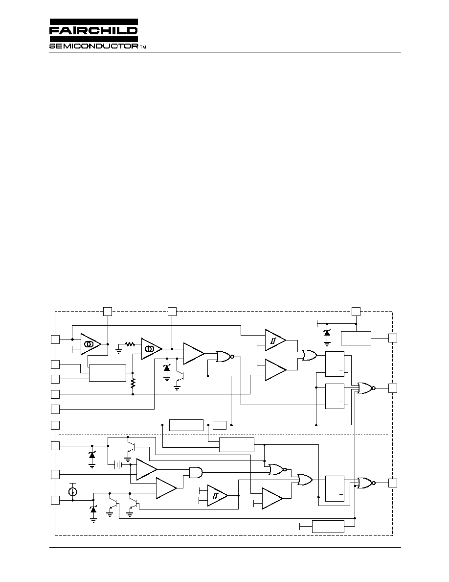
Block Diagram
15
VEAO
IEAO
VFB
IAC
VRMS
ISENSE
RAMP 1
OSCILLATOR
OVP
PFC ILIMIT
UVLO
VREF
PULSE WIDTH MODULATOR
POWER FACTOR CORRECTOR
2.5V
+
-
-
+
16
2
4
3
7.5V
REFERENCE
14
VCC
13
VCCZ
VEA
8
-
+
IEA
1
+
-
+
-
PFC OUT
12
S
R
Q
Q
S
R
Q
Q
2.7V
-1V
RAMP 2
9
PWM OUT
11
S
R
Q
Q
VDC
6
SS
5
RTCT
7
VCC
DUTY CYCLE
LIMIT
+
-
1V
-
+
2.5V
VFB
-
+
8V
8V
VIN OK
GAIN
MODULATOR
VCCZ
÷2
3.5k
3.5k
1.25V
50
µA
-
+
13.5V
DC ILIMIT
8V
ML4841
Variable Feedforward PFC/PWM Controller Combo
ML4841
PRODUCT SPECIFICATION
2
REV. 1.0.3 6/13/01
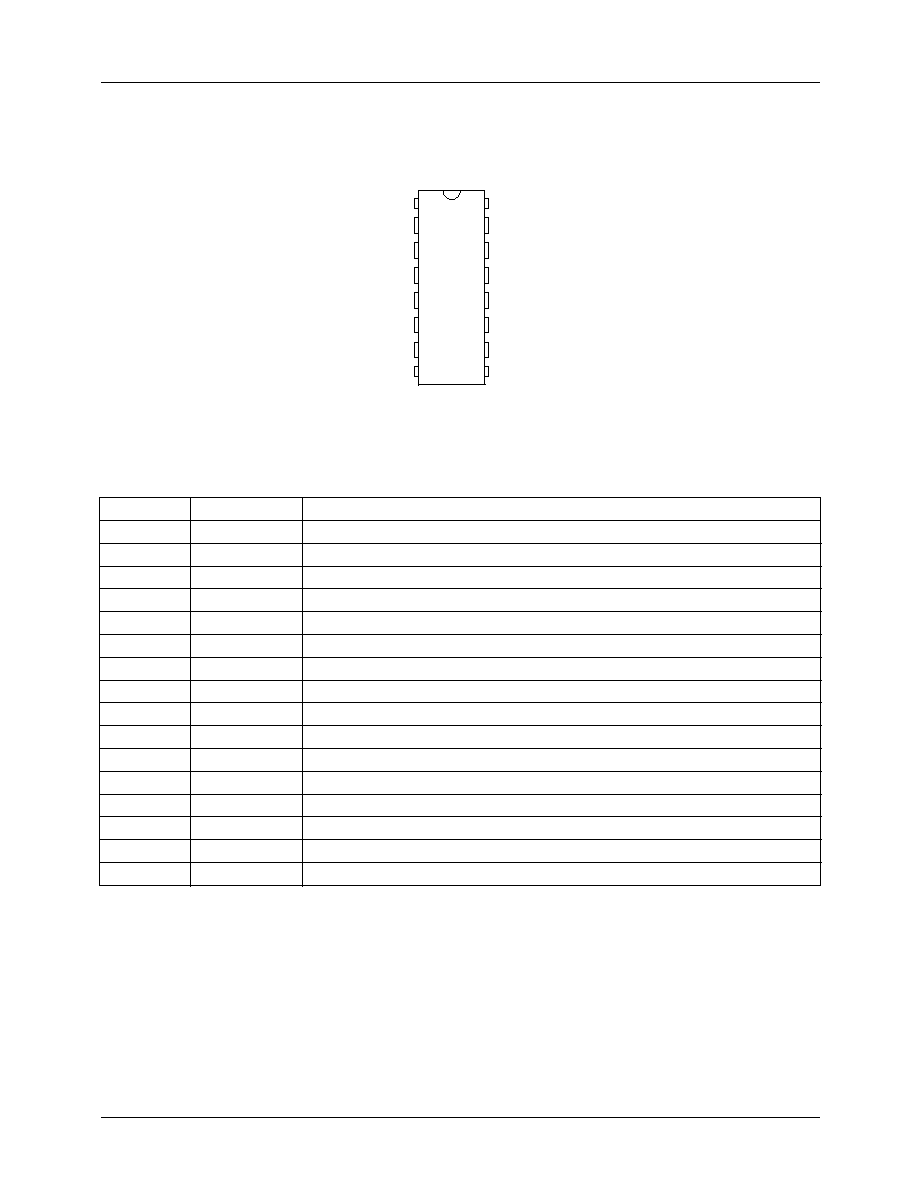
Pin Configuration
Pin Description
PIN NAME
FUNCTION
1
IEAO
PFC transconductance current error amplifier output
2
I
AC
PFC gain control reference input
3
I
SENSE
Current sense input to the PFC current limit comparator
4
V
RMS
Input for PFC RMS line voltage compensation
5
SS
Connection point for the PWM soft start capacitor
6
V
DC
PWM voltage feedback input
7
R
T
C
T
Connection for oscillator frequency setting components
8
RAMP 1
PFC ramp input
9
RAMP 2
PWM ramp current sense input
10
GND
Ground
11
PWM OUT
PWM driver output
12
PFC OUT
PFC driver output
13
V
CC
Positive supply (connected to an internal shunt regulator).
14
V
REF
Buffered output for the internal 7.5V reference
15
V
FB
PFC transconductance voltage error amplifier input
16
VEAO
PFC transconductance voltage error amplifier output
1
2
3
4
5
6
7
8
16
15
14
13
12
11
10
9
IEAO
IAC
ISENSE
VRMS
SS
VDC
RT/CT
RAMP 1
VEAO
VFB
VREF
VCC
PFC OUT
PWM OUT
GND
RAMP 2
TOP VIEW
ML4841
16-Pin PDIP (P16)
PRODUCT SPECIFICATION
ML4841
REV. 1.0.3 6/13/01
3
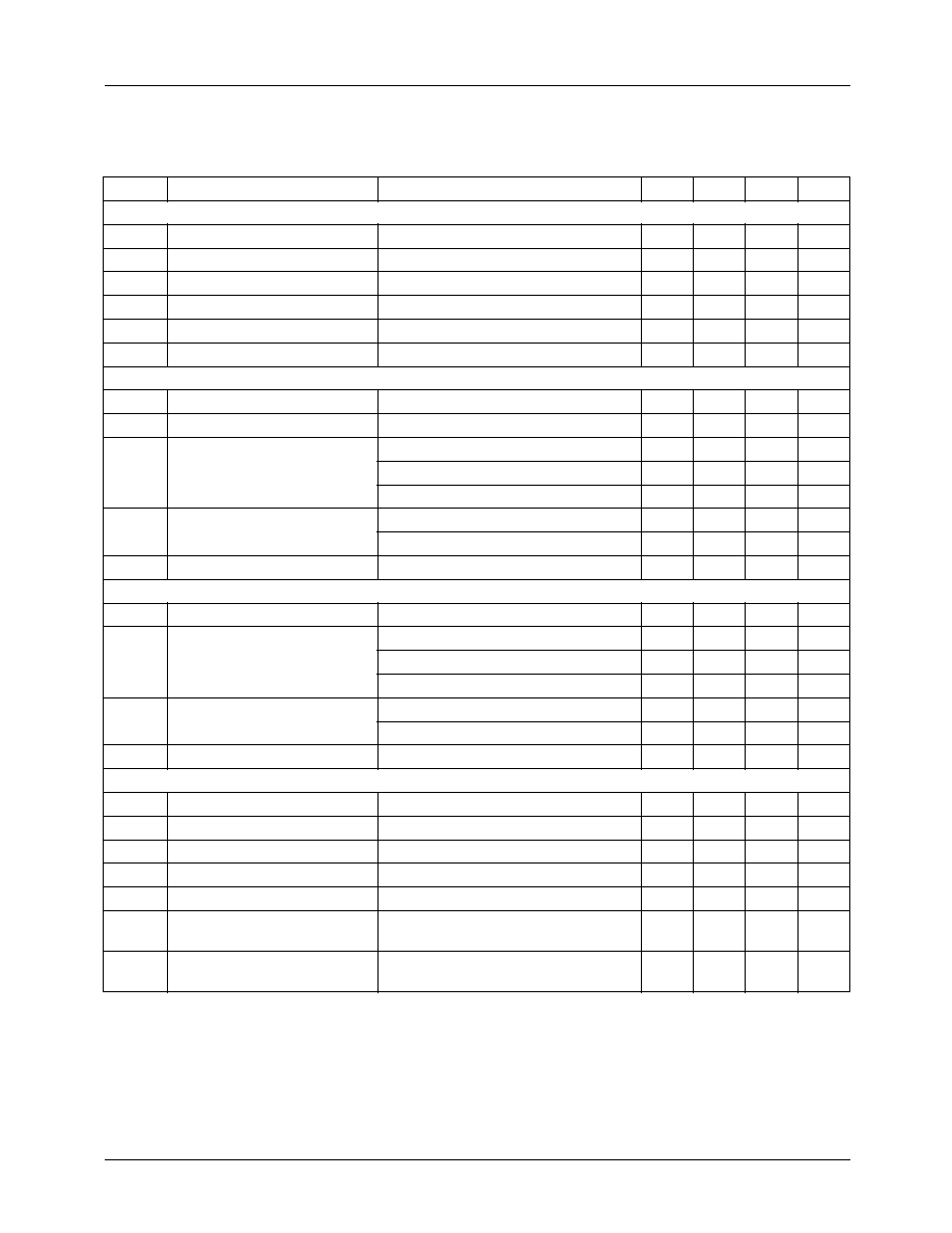
Absolute Maximum Ratings
Absolute maximum ratings are those values beyond which the device could be permanently damaged. Absolute maximum
ratings are stress ratings only and functional device operation is not implied.
Operating Conditions
Temperature Range
Parameter
Min.
Max.
Units
V
CC
Shunt Regulator Current
55
mA
I
SENSE
Voltage
-3
5
V
Voltage on Any Other Pin
GND - 0.3
V
CCZ
+ 0.3
V
I
REF
20
mA
I
AC
Input Current
10
mA
Peak PFC OUT Current, Source or Sink
500
mA
Peak PWM OUT Current, Source or Sink
500
mA
PFC OUT, PWM OUT Energy Per Cycle
1.5
mJ
Junction Temperature
150
°C
Storage Temperature Range
65
150
°C
Lead Temperature (Soldering, 10 sec)
260
°C
Thermal Resistance (
JA
)
Plastic DIP
80
°C/W
Parameter
Min.
Max.
Units
ML4841CP
0
70
°C
Electrical Characteristics
Unless otherwise specified, I
CC
= 25mA, R
T
= 23k
, R
RAMP1
= 28.7k
, C
T
= 400pF, C
RAMP1
= 270pF, T
A
=
Operating Temperature Range (Note 1)
Symbol
Parameter
Conditions
Min.
Typ.
Max.
Units
Voltage Error Amplifier
Input Voltage Range
0
7
V
Transconductance
V
NON INV
= V
INV
, VEAO = 3.75V
40
70
100
µ
Feedback Reference Voltage
2.4
2.5
2.6
V
Input Bias Current
Note 2
-0.5
-1.0
µA
Output High Voltage
6.0
6.7
V
Output Low Voltage
0.65
1.0
V
Source Current
V
IN
= ±0.5V, V
OUT
= 6V
-40
-90
µA
Sink Current
V
IN
= ±0.5V, V
OUT
= 1.5V
40
90
µA
Open Loop Gain
60
75
dB
PSRR
V
CCZ
- 3V < V
CC
< V
CCZ
- 0.5V
60
75
dB
Current Error Amplifier
Input Voltage Range
-1.5
2
V
Transconductance
V
NON INV
= V
INV
, VEAO = 3.75V
130
195
310
µ
Input Offset Voltage
±3
±15
mV
ML4841
PRODUCT SPECIFICATION
4
REV. 1.0.3 6/13/01
Input Bias Current
-0.5
-1.0
µA
Output High Voltage
6.0
6.7
V
Output Low Voltage
0.65
1.0
V
Source Current
V
IN
= ±0.5V, V
OUT
= 6V
-40
-90
µA
Sink Current
V
IN
= ±0.5V, V
OUT
= 1.5V
40
90
µA
Open Loop Gain
60
75
dB
PSRR
V
CCZ
- 3V < V
CC
< V
CCZ
- 0.5V
60
75
dB
OVP Comparator
Threshold Voltage
2.6
2.7
2.8
V
Hysteresis
70
95
125
mV
PFC I
LIMIT
Comparator
Threshold Voltage
-0.8
-1.0
-1.15
V
(PFC I
LIMIT
V
TH
- Gain
Modulator Output)
100
190
mV
Delay to Output
150
300
ns
DC I
LIMIT
Comparator
Threshold Voltage
0.9
1.0
1.1
V
Input Bias Current
±0.3
±1
µA
Delay to Output
150
300
ns
V
IN
OK Comparator
Threshold Voltage
2.4
2.5
2.6
V
Hysteresis
0.8
1.0
1.2
V
Gain Modulator
Gain (Note 3)
I
AC
= 100µA, V
RMS
= V
FB
= 0V
0.35
0.50
0.65
I
AC
= 50µA, V
RMS
= 1.2V, V
FB
= 0V
1.15
1.65
2.15
I
AC
= 50µA, V
RMS
= 1.8V, V
FB
= 0V
0.52
0.74
0.96
I
AC
= 100µA, V
RMS
= 3.3V, V
FB
= 0V
0.14
0.20
0.26
Bandwidth
IAC = 100µA
10
MHz
Output Voltage
I
AC
= 250µA, V
RMS
= 1.15V,
V
FB
= 0V
0.74
0.82
0.90
V
Oscillator
Initial Accuracy
T
A
= 25°C
188
200
212
kHz
Voltage Stability
V
CCZ
- 3V < V
CC
< V
CCZ
- 0.5V
1
%
Temperature Stability
2
%
Total Variation
Line, Temp
182
218
kHz
Ramp Valley to Peak Voltage
2.5
V
Dead Time
PFC Only
260
400
ns
C
T
Discharge Current
V
RAMP 2
= 0V, V
RAMP 1
= 2.5V
4.5
7.5
9.5
mA
Electrical Characteristics
(continued)
Unless otherwise specified, I
CC
= 25mA, R
T
= 23k
, R
RAMP1
= 28.7k
, C
T
= 400pF, C
RAMP1
= 270pF, T
A
=
Operating Temperature Range (Note 1)
Symbol
Parameter
Conditions
Min.
Typ.
Max.
Units
PRODUCT SPECIFICATION
ML4841
REV. 1.0.3 6/13/01
5
Notes
1. Limits are guaranteed by 100% testing, sampling, or correlation with worst-case test conditions.
2. Includes all bias currents to other circuits connected to the V
FB
pin.
3. Gain = K x 5.3V; K = (I
GAINMOD
- I
OFFSET
) x I
AC
x (VEAO - 1.5V)
-1
.
Reference
Output Voltage
T
A
= 25°C, I(V
REF
) = 1mA
7.4
7.5
7.6
V
Line Regulation
V
CCZ
- 3V < V
CC
< V
CCZ
- 0.5V
2
10
mV
Load Regulation
1mA < I(V
REF
) < 20mA
2
15
mV
Temperature Stability
0.4
%
Total Variation
Line, Load, Temp
7.25
7.65
V
Long Term Stability
T
J
= 125°C, 1000 Hours
5
25
mV
PFC
Minimum Duty Cycle
V
IEAO
> 6.7V
0
%
Maximum Duty Cycle
V
IEAO
< 1.2V
90
95
%
Output Low Voltage
I
OUT
= -20mA
0.4
0.8
V
I
OUT
= -100mA
0.7
2.0
V
I
OUT
= 10mA, V
CC
= 8V
0.8
1.5
V
Output High Voltage
I
OUT
= 20mA
10
10.5
V
I
OUT
= 100mA
9.5
10
V
Rise/Fall Time
C
L
= 1000pF
50
ns
PWM
DC
Duty Cycle Range
0-44
0-47
0-50
%
V
OL
Output Low Voltage
I
OUT
= -20mA
0.4
0.8
V
I
OUT
= -100mA
0.7
2.0
V
I
OUT
= 10mA, V
CC
= 8V
0.8
1.5
V
V
OH
Output High Voltage
I
OUT
= 20mA
10
10.5
V
I
OUT
= 100mA
9.5
10
V
Rise/Fall Time
C
L
= 1000pF
50
ns
Supply
V
CCZ
Shunt Regulator Voltage
12.8
13.5
14.2
V
V
CCZ
Load Regulation
25mA < I
CC
< 55mA
±100
±200
mV
V
CCZ
Total Variation
Load, Temp
12.4
14.6
V
Start-up Current
V
CC
= 11.2V, C
L
= 0
0.7
1.0
mA
Operating Current
V
CC
< V
CCZ
- 0.5V, C
L
= 0
17
21
mA
Undervoltage Lockout
Threshold
V
CCZ
-
1.0
V
CCZ
-
0.7
V
CCZ
-
0.4
V
Undervoltage Lockout
Hysteresis
2.7
3.0
3.3
V
Electrical Characteristics
(continued)
Unless otherwise specified, I
CC
= 25mA, R
T
= 23k
, R
RAMP1
= 28.7k
, C
T
= 400pF, C
RAMP1
= 270pF, T
A
=
Operating Temperature Range (Note 1)
Symbol
Parameter
Conditions
Min.
Typ.
Max.
Units