 | –≠–ª–µ–∫—Ç—Ä–æ–Ω–Ω—ã–π –∫–æ–º–ø–æ–Ω–µ–Ω—Ç: ML4854IT | –°–∫–∞—á–∞—Ç—å:  PDF PDF  ZIP ZIP |
www.fairchildsemi.com
REV. 1.0.7 5/6/03
Features
∑ 95% Efficiency at 200mA Load Current
∑ Integrated Peak Current Limit
∑ Variable Output Voltage Determined by External Resistors
∑ Variable On-time Pulse Frequency Modulation (PFM)
∑ Fully Internal Synchronous Rectifier (no external diodes)
for High Efficiency and Low Peak Currents
∑ Low-Battery Detection
∑ Logic Controlled Shutdown with True Load Disconnect
Applications
∑ 2-3 alkaline/NiMH cells or 1 Li-Ion cell Operated Devices
∑ Cell Phones
∑ Medical Devices
∑ PDAs
∑ Portable Instrumentation
General Description
The ML4854 is a low power boost regulator designed for
low voltage DC to DC conversion in two-cell battery pow-
ered systems such as cell phones and PDAs. The converter
starts up at 1.3V and has an operating input voltage range
from 1.6V to 4.5V. After the start it operates at an input
voltage as low as 0.8V. Output voltage can be adjusted by
external resistors from 3.3V to 5V with a maximum load
current of 0.5A.
Quiescent current in shut down mode is less than 30µA,
which maximizes the battery live time. The ON time changes
with the input voltage to maintain the ripple current constant
and to provide the highest efficiency over a wide load range,
while maintaining low peak currents in the boost inductor.
The combination of integrated synchronous rectification,
variable frequency operation, and low supply current make
ML4854 ideal for portable applications.
The ML4854 is available in an 8 lead TSSOP package.
ML4854
Adjustable, Low-Current, 2-Cell Boost Regulator
with Shutdown and Low Battery Detect
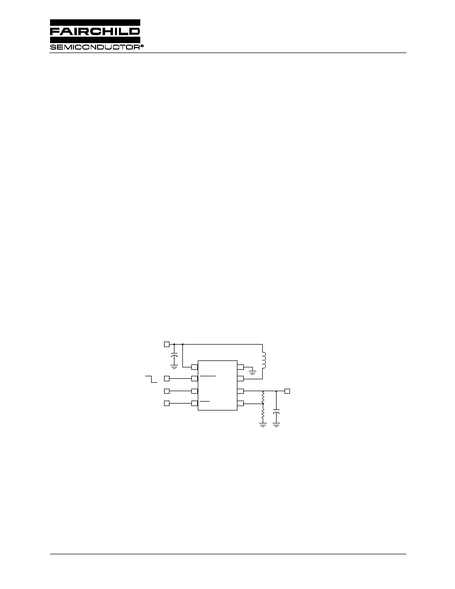
Typical Application
V
IN
Input 1.6V
to 4.5V
On
Off
Low Battery
Detect In
Output 3.3V to 5V
up to 0.5A
ML4854
Low Battery
Detect Out
SHDN
LBI
LB0
GND
V
L
V
OUT
FB
1
2
3
4
8
7
6
5
PRODUCT SPECIFICATION
ML4854
2
REV. 1.0.7 5/6/03
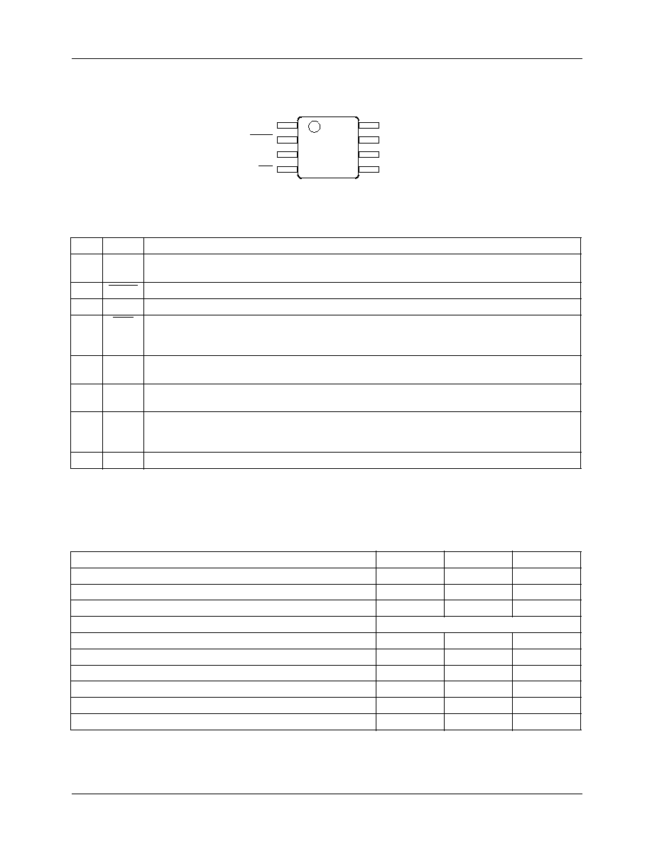
Pin Configuration
Pin Description
Absolute Maximum Ratings
Absolute maximum ratings are those values, beyond which the device could be permanently damaged. Absolute maximum
ratings are stress ratings only and functional device operation is not implied.
PIN
NAME
FUNCTION
1
V
IN
Battery Input Voltage
. Supplies the IC during start-up. After the output is running, the IC draws
power from V
OUT
.
2
SHDN
Shut Down
. Pulling this pin low shuts down the regulator, isolating the load from the input.
3
LBI
Low-Battery Input
. Pulling this pin below a threshold causes the LBO pin to go low.
4
LBO
Low-Battery Output
. This pin provides an active low signal to alert the user when the LBI
voltage falls below its targeted value. The open-drain output can be used to reset a
microcontroller.
5
FB
Programming Feedback Pin
. Sets the output voltage. This pin is used to adjust the output
voltage via a resistive divider from V
OUT
.
6
V
OUT
Boost regulator output
. Output voltage can be set to be in the 3 to 5V range. Startup at
moderate load is achievable at input voltages around 1.25V.
7
V
L
Boost inductor connection
. An inductor is connected between this pin and V
IN
. When servicing
the output supply, this pin pulls low, charging the inductor, then shuts off dumping the energy
through the synchronous rectifier to the output.
8
GND
Ground of the IC
.
Parameter Min.
Max.
Units
V
IN
,
V
OUT
Voltages (Relative to GND)
-0.3
7
V
Switch Voltage (V
L
to GND)
-0.3
V
OUT
+0.3
V
Voltage on any other Pin
-0.3
V
OUT
+0.3
V
Peak Switch Current (Ipeak)
-- Internally Limited --
Output Current (I
OUT
)
500
mA
Continuous Power Dissipation
320
mW
Thermal Resistance (
JA
)
124
∞C/W
Junction Temperature
150
∞C
Storage Temperature Range
-65
+165
∞C
Lead Temperature (soldering, 10s)
300
∞C
V
IN
GND
V
L
V
OUT
FB
1
2
3
4
8
7
TOP VIEW
8-Lead TSSOP (T08)
6
5
SHDN
LBI
LB0
ML4854
PRODUCT SPECIFICATION
REV. 1.0.7 5/6/03
3
Recommended Operating Conditions
Electrical Characteristics
Unless otherwise specified, V
IN
=1.6V to 3V, I
LOAD
=1mA, T
A
=-40∞C to +85∞C. Test Circuit Fig.1. Typical values are
at T
A
= +25∞C
Parameter
Min.
Max.
Units
Temperature Range
-40
+85
∞C
V
IN
Operating Range
1.6
0.9 V
OUT
V
V
OUT
Operating Range
3.0
5.0
V
Parameter
Conditions
Min.
Typ.
Max.
Units
Start Up Voltage
I
LOAD
<1mA
1.25
1.5
V
Operating Voltage
After start I
LOAD
=10mA, V
OUT
=3.3V/5V
0.8
V
Output Voltage
V
OUT
(nom.)=3.3V
V
OUT
(nom.)=5V
3.15
4.775
3.3
5
3.45
5.225
V
V
Output Voltage Adjust Range
3
5
V
Steady State Output Current
(see diagram)
V
OUT
=3.3V, V
IN
=2.5V
500
mA
V
OUT
=5V, V
IN
=2.5V
330
mA
Pulse Width
V
IN
= 3V
0.8
1.32
1.9
µ
s
V
IN
= 2.4V
1.2
1.64
2.3
µ
s
V
IN
= 1.8V
1.8
2.15
3.1
µ
s
V
IN
= 1.5V
2.2
2.57
4.0
µ
s
Minimum Off-Time
0.5
µ
s
Line Regulation
V
IN
=1.6V to 3V, I
OUT
=2mA, V
OUT
=3.3V
0.5
%
V
OUT
=5V
0.5
%
Load Regulation
0 to 250mA V
IN
=2.4V ,V
OUT
=3.3V
1.0
%
0 to 150mA V
IN
=2.4V ,V
OUT
=5V
1.0
%
Feedback Voltage (VFB)
1.230
V
LBI Threshold Voltage
0.390
V
LBI Hysteresys
25
mV
Internal NFET, PFET ON Resist.
I
LOAD
= 100mA
275
m
Efficiency
(I
LOAD
=200mA) V
IN
=3V, V
OUT
= 3.3V
95
%
Quiescent Current ≠ SHDN
SHDN=0V, R1 excluded,V
IN
=3V
26
100
µ
A
SHDN=3V, R1 excluded,V
IN
=3V
85
200
µ
A
LBO Output Voltage
V
LBI
= 0, I
SINK
=1mA
0.2
V
SHDN Input Voltage @V
IN
=3V V
OUT
=3.3V/5V
1.6
V
SHDN Input Voltage @V
IN
=1.6V
V
OUT
=3.3V/5V
0.8
V
PRODUCT SPECIFICATION
ML4854
4
REV. 1.0.7 5/6/03
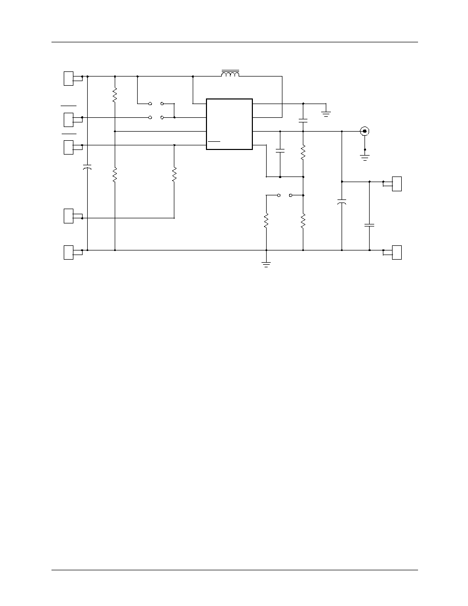
Figure 1. Test Circuit
SHDN
L1
C5
0.1uF
JP3
R6
287K
1
2
C4
1.0uF
1
2
10V
GND1
1
2
1
2
1
2
U1 ML4854
1
2
3
4
5
6
7
8
Vin
Shut down
LBI
LBO
FB
Vout
VL
Gnd
+
C3
18pF
R1
750K
R2
240K
R3
100K
C1
47
µF
UP1B100
+ C2
47uF
VOUT
3.3V to 5.0V
1
2
R5
240K
JP1
1
2
JP2
R4
402K
J1
SCOPE JACK
10uH
Reset
VIN
1.6V to 3.0V
Ext
Pull Up
GND
ML4854
PRODUCT SPECIFICATION
REV. 1.0.7 5/6/03
5
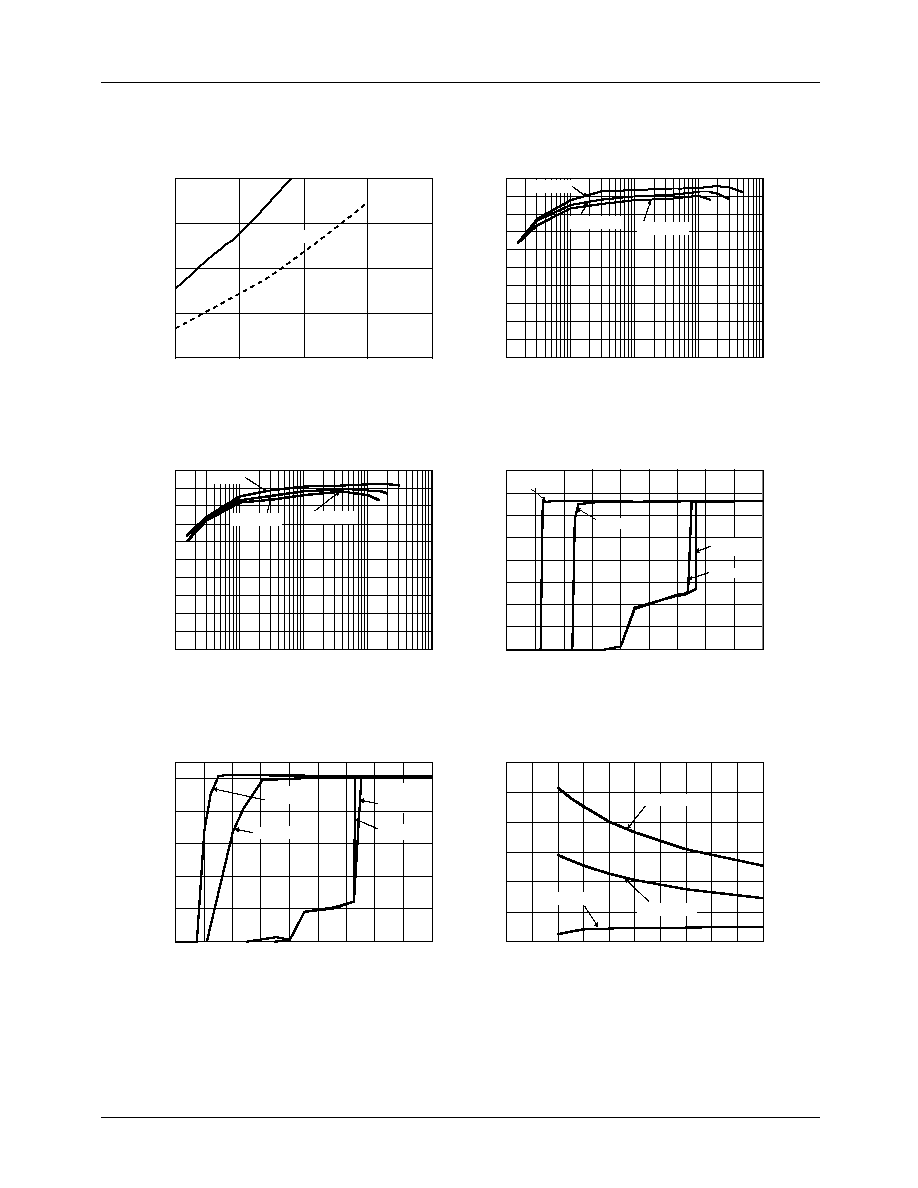
Typical Operating Characteristics
(L=10µH, C
IN
=47µF, C
OUT
=47µF//1.0µF T=25∞C)
Maximum Steady State Load
Current vs. Input Voltage
100
200
300
400
500
1.5
2
2.5
3
Input Voltage, V
Max.Load Current, mA
V
OUT
=
5V
V
OUT
=
3.3V
Efficiency vs. Load Current
Vout = 3.3V
0.0
10.0
20.0
30.0
40.0
50.0
60.0
70.0
80.0
90.0
100.0
0.1
1
10
100
1000
Output Current, mA
Efficiency, %
0.0
10.0
20.0
30.0
40.0
50.0
60.0
70.0
80.0
90.0
100.0
0.1
1
10
100
1000
Output Current, mA
Efficiency, %
Efficiency vs. Load Current
Vout = 5V
Starting Up and Turning Off VOUT=3.3V
Iload=10mA/50mA
0
0.5
1
1.5
2
2.5
3
3.5
4
0
0.2
load=50mA
load=50mA
TURN OFF:
START UP
Iload=50mA
START UP:
Iload=50mA
Iload=10mA
Iload=10mA
Iload=10mA
TURN OFF:
Iload=10mA
0.4
0.6
0.8
1.0
1.2
1.4
1.6
1.8
Input (Battery) Voltage, V
Output Voltage, V
Starting Up and turning Off VOUT=5V
Iload=10mA/50mA
0
1
2
3
4
5
0
0.2
0.4
0.6
0.8
1
1.2
1.4
1.6
1.8
Input (Battery) Voltage, V
0
1.2 1.4 1.6 1.8
2
2.2 2.4 2.6 2.8 3.0
Battery Voltage, V
Output Voltage, V
Battery Current,
µ
A
No-Load Battery Current vs. Input Battery
Voltage
0
50
100
150
200
250
300
Vin=2.0V
Vin=3V
Vin=1.5V
Vin=3V
Vin=2.0V
Vin=1.5V
Vout=5V
Vout=3.3V
Shut Down