www.fairchildsemi.com
REV. 1.0.2 8/10/01
Features
∑ Guaranteed full load start-up and operation at 1.8V input
∑ Continuous conduction mode for high output current
∑ Very low quiescent current
∑ Pulse frequency modulation and internal synchronous
rectification for high efficiency
∑ Maximum switching frequency > 200kHz
∑ Minimum external components
∑ Low ON resistance internal switching FETs
∑ Fixed 12V output can be adjusted to lower output voltages
General Description
The ML4865 is a high voltage, continuous conduction boost
regulator designed for DC to DC conversion in multiple cell
battery powered systems. Continuous conduction allows the
regulator to maximize output current for a given inductor.
The maximum switching frequency can exceed 200kHz,
allowing the use of small, low cost inductors. The ML4865 is
capable of start-up with input voltages as low as 1.8V and
generates a 12V output with output voltage accuracy of ±4%.
Unlike most boost regulators, the ML4865 isolates the load
from the battery when the SHDN pin is high. An integrated
synchronous rectifier eliminates the need for an external
Schottky diode and provides a lower forward voltage drop,
resulting in higher conversion efficiency. In addition, low
quiescent battery current and variable frequency operation
result in high efficiency even at light loads. The ML4865
requires only one inductor and two capacitors to build a very
small regulator circuit capable of achieving conversion effi-
ciencies approaching 90%.
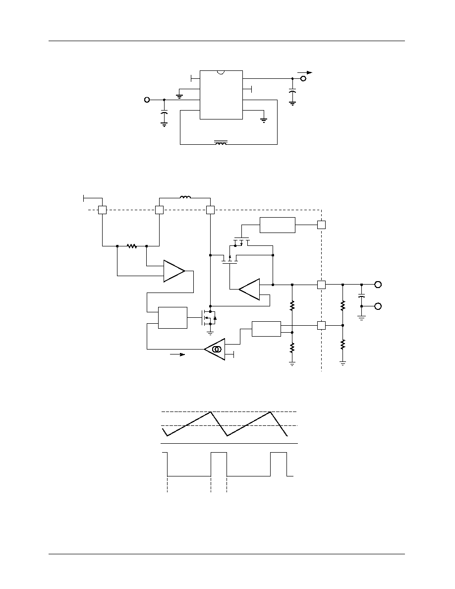
Block Diagram
VL2
8
VOUT
1
SENSE
6
+
≠
SHUTDOWN
CONTROL
7
SHDN
VIN
3
2.42V
START-UP
2
GND
VL1
4
SYNCHRONOUS
RECTIFIER
CONTROL
BOOST
CONTROL
SHDN
+
≠
+
≠
5
PWR GND
FEEDBACK
CONTROL
ML4865
High Voltage High Current Boost Regulator
ML4865
PRODUCT SPECIFICATION
2
REV. 1.0.2 8/10/01
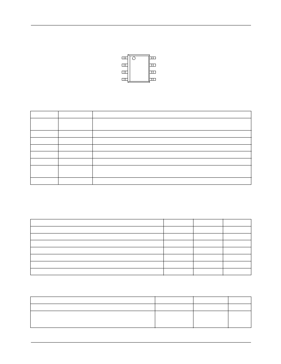
Pin Configuration
Pin Description
Absolute Maximum Ratings
Absolute Maximum Ratings are those values, beyond which the device could be permanently damaged. Absolute maximum
ratings are stress ratings only and functional device operation is not implied.
Operating Conditions
PIN NAME
FUNCTION
1
SENSE
Programming pin for setting the output to any value lower than the normal fixed
voltage.
2
GND
Ground.
3
V
IN
Battery input voltage.
4
V
L1
Boost inductor connection.
5
PWR GND
Return for the internal power transistors.
6
V
L2
Boost inductor connection.
7
SHDN
Pulling this pin to V
IN
through an external resistor shuts down the regulator,
isolating the load from the input.
8
V
OUT
Boost regulator output.
Parameter
Min.
Max.
Units
Voltage on any other Pin
GND ≠ 0.3
16.5
V
Peak Switch Current (I
PEAK
) 2
A
Average Switch Current (I
AVG
)
1
A
Junction Temperature
150
∞C
Storage Temperature Range
-65
150
∞C
Lead Temperature (soldering, 10s)
150
∞C
Thermal Resistance (
JA
)
160
∞C/W
Parameter
Min.
Max.
Units
Temperature Range ML4865CS-2
0
70
∞C
V
IN
Voltage Range
Without external rectifier
With external rectifier
1.8
1.8
6
10
V
V
ML4865
8-Pin SOIC (S08)
1
2
3
4
8
7
6
5
SENSE
GND
VIN
VL1
VOUT
SHDN
VL2
PWR GND
TOP VIEW

PRODUCT SPECIFICATION
ML4865
REV. 1.0.2 8/10/01
5
Functional Description
The ML4865 combines a unique form of current mode con-
trol with a synchronous rectifier to create a boost converter
that can deliver high currents while maintaining high effi-
ciency. Current mode control allows the use of a very small,
high frequency inductor and output capacitor. Synchronous
rectification replaces the conventional external Schottky
diode with an on-chip PMOS FET to reduce losses, eliminate
an external component, and allows for load disconnect. Also
included on-chip are an NMOS switch and current sense
resistor, further reducing the number of external components,
which makes the ML4865 very easy to use.
Regulator Operation
The ML4865 is a variable frequency, current mode switching
regulator. Its unique control scheme converts efficiently over
more than three decades of load current. A detailed block
diagram of the boost converter is shown in Figure 2.
Error amplifier A3 converts deviations in the desired output
voltage to a small current, I
SET
. The inductor current is mea-
sured through a 150m
resistor which is amplified by A1.
The boost control block matches the average inductor current
to a multiple of the I
SET
current by switching Q1 on and off.
The peak inductor current is limited by the controller to
about 1.2A.
At light loads, I
SET
will momentarily reach zero after an
inductor discharge cycle causing Q1 to stop switching.
Depending on the load, this idle time can extend to tenths of
seconds. While the circuit is not switching, only 25µA of
supply current is drawn from the output. This allows the part
to remain efficient even when the load current drops below
250µA.
Amplifier A2 and the PMOS transistor Q2 work together to
form a low drop diode. When transistor Q1 turns off, the cur-
rent flowing in the inductor causes pin 6 to go high. As the
voltage on V
L2
rises above V
OUT
, amplifier A2 allows the
PMOS transistor Q2 to turn on. In discontinuous operation,
(where I
L
always returns to zero), A2 uses the resistive drop
across the PMOS switch Q2 to sense zero inductor current
and turns the PMOS switch off. In continuous operation, the
PMOS turn off is independent of A2 and is determined by the
boost control circuitry.
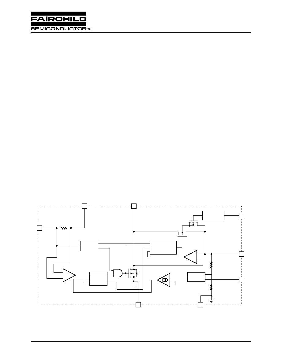
Typical inductor current and voltage waveforms are shown in
Figure 3.
Shutdown
The SHDN pin should be held low for normal operation.
Raising the shutdown voltage above the threshold level will
disable the synchronous rectifier, Q2 and Q3, and force I
SET
to zero. This prevents switching from occurring and
disconnects the body diode of Q2 from the output. As a
result, the output voltage is allowed to drop below the input
voltage and current is prevented from flowing from the input
to the output.
Feedback
The SENSE pin should be left open or bypassed to ground
for normal operation. The addition of the resistor divider R1
and R2 causes the input of error amplifier A3 to reach the
threshold voltage before the internal resistors do. This
allows the ML4865 to provide output voltages lower than the
preset 12V if desired.
Design Considerations
Input Voltage Range
The input voltage range determines whether an external
Schottky diode is necessary or optional. If the input voltage
is 6V or lower, the ML4865 can be operated as a stand alone
boost regulator with a shutdown that fully isolates the input
from the output. Adding an optional Schottky diode extends
the input voltage range up to 10V, and improves the effi-
ciency and the output current capability. However, the exter-
nal diode now provides a leakage path from the input to the
output during shutdown.
Output Current Capability
The maximum current available at the output of the regulator
is related to the maximum inductor current by the ratio of the
input to output voltage and the full load efficiency. The max-
imum inductor current is dependent on the input voltage.
The full load efficiency may be as low as 65% when the
ML4865 is used without a Schottky diode and can exhibit an
input voltage dependence when an external diode is used.
The maximum output current can be determined by using the
typical performance curves shown in Figures 4 and 5, or by
calculation using the following empirical equation:
Where, for applications using the internal synchronous
rectifier:
And for applications using an external Schottky:
I
V
V
I
OUT MAX
IN
OUT
IN
(
)
◊
◊ (A)
(1)
I
V
(
(
(
(
V
V
OUT MAX
IN
OUT
IN
(
)
.
.
.
◊
◊
+
◊
0 05
0 4
0 65
I
V
IN
IN
=
◊
+
0 05
0 4
.
.
= 0 65
.
(
(
I
V
V
V
V
OUT MAX
IN
OUT
IN
IN
(
)
.
.
.
.
◊
◊
+
◊
◊
+
0 07
0 4
0 025
0 65
(
(
(
(
(
(
(
(
(
(
(
(
I
V
IN
IN
=
◊
+
0 07
0 4
.
.
=
◊
+
0 025
0 65
.
.
V
IN