 | ÐлекÑÑоннÑй компоненÑ: ML6427CS | СкаÑаÑÑ:  PDF PDF  ZIP ZIP |
Äîêóìåíòàöèÿ è îïèñàíèÿ www.docs.chipfind.ru
August 1999
PRELIMINARY
ML6427
75
W Quad Video Cable Drivers and Filters
with Switchable Inputs
1
GENERAL DESCRIPTION
The ML6427 is a quad 4
th
-order Butterworth lowpass
reconstruction filter plus quad video amplifier optimized
for minimum overshoot and flat group delay. Each filter
channel has a two-input multiplexer that switches between
two groups of quad video signals. Applications driving
SCART and EVC cables are supported for composite,
component, and RGB video.
1V
P-P
input signals from DACs are AC coupled into the
ML6427 where they are DC restored. Outputs are AC
coupled and drive 2V
P-P
into a 150
W load. The ML6427
can provide DC coupled outputs for certain applications.
A fifth unfiltered channel is provided to support an
additional analog composite video input. A swapping
multiplexer between the two composite channels allows
the distribution amplifiers to output from either input.
Several ML6427s can be arranged in a master-slave
configuration where an external sync can be used for CV
and RGB outputs.
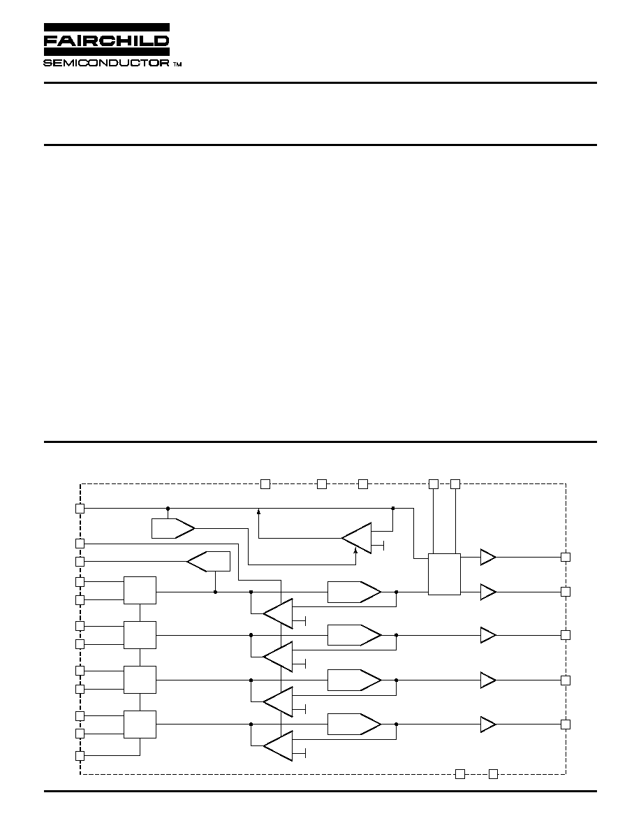
BLOCK DIAGRAM
FEATURES
s
Cable drivers for Peritel (SCART), Enhanced Video
Connector (EVC), and standard video connectors, 75
W
cable drivers for CV, S-video, and RGB
s
7.1MHz CV, RGB, and S-video, NTSC or PAL filters
with mux inputs and output channel mux
s
Quad reconstruction filter or dual anti-aliasing filter
s
43dB stopband attenuation at 27MHz
s
1dB flatness up to 4.8MHz
s
12ns group delay flatness up to 10MHz
s
0.4% differential gain, 0.4º differential phase on all
channels
s
0.4% total harmonic distortion on all channels
s
Master-slave configuration allows up to 8 multiplexed,
filtered output signals
A/B MUX
1
12
BINA/C1
BINB/C2
BOUT/COUT
GND
GNDO
11
GINB/Y2
10
GINA/Y6
9
RINB/Y5
8
RINA/Y4
7
CVINFB/Y3*
4
CVINFA/Y2*
3
SYNCOUT
MUX
MUX
MUX
SWAP
MUX
MUX
15
GOUT/YOUTD
16
ROUT/YOUTC
18
CVOUT/YOUTB
20
CVOUT1/YOUTA
21
5
19
4th-ORDER
FILTER
TRANSCONDUCTANCE
ERROR AMP
TRANSCONDUCTANCE
ERROR AMP
UNFILTERED CHANNEL
SWAP CVF
SWAP CVU
VCC
VCCOCV
REQUIRED
SYNC STRIP
SYNC
TIMER
SYNC
TIMER
24
22
VCCORGB
17
6
13
14
SYNCIN
23
SYNCIN
2
+
0.5V
+
0.5V
4th-ORDER
FILTER
TRANSCONDUCTANCE
ERROR AMP
+
0.5V
4th-ORDER
FILTER
TRANSCONDUCTANCE
ERROR AMP
+
0.5V
4th-ORDER
FILTER
TRANSCONDUCTANCE
ERROR AMP
*CAN ALSO INPUT SYNC ON GREEN SIGNALS
+
0.75V
×
2
×
2
×
2
×
2
×
2
ML6427
2
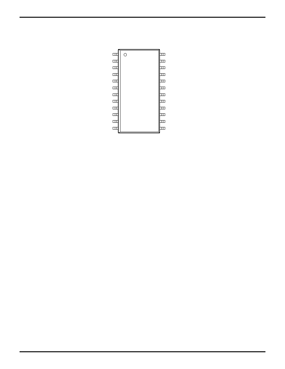
PIN CONFIGURATION
1
2
3
4
5
6
7
8
9
10
11
12
24
23
22
21
20
19
18
17
16
15
14
13
A/B MUX
CVINU/Y1
CVINFA/Y2
CVINFB/Y3
GND
VCC
RINA/Y4
RINB/Y5
GINA/Y6
GINB/Y7
BINA/C1
BINB/C2
SYNCOUT
SYNCIN
VCCOCV
CVOUT1/YOUTA
CVOUT2/YOUTB
GNDO
ROUT/YOUTC
VCCORGB
GOUT/YOUTD
BOUT/COUT
SWAP CVU
SWAP CVF
TOP VIEW
ML6427
24-Pin SOIC (S24)

ML6427
3
PIN DESCRIPTION
PIN
NAME
FUNCTION
1
A/
B
MUX
Logic input pin to select between
Bank <A> or <B> of the CV, RGB,
or Y/C inputs. Internally pulled high.
2
CV
INU
/Y1
Unfiltered analog composite video
or luma video input. Internally
pulled high. A composite or luma or
green signal must be present on
either the CV
INF
A/Y2 or the CV
INF
B/
Y3 input to provide necessary sync
signals to other channels (R, G, B, Y,
C). Otherwise, sync must be
provided at SYNCIN. For RGB
applications the green channel with
sync can be used as an input to this
pin (see RGB Applications section).
3
CV
INF
A/Y2
Filtered analog composite video or
luma video input for Bank <A>.
Note that SYNC is stripped from this
signal for the other channels. A
composite or luma or green signal
must be present on either the
CV
INF
A/Y2 or the CV
INF
B/Y3 input
to provide necessary sync signals to
other channels (R, G, B, Y, C).
Otherwise, sync must be provided
at SYNCIN. For RGB applications
the green channel with sync can be
used as an input to this pin (see
RGB Applications section).
4
CV
INF
B/Y3
Filtered analog composite video or
luma video input for Bank <B>.
Note that SYNC is stripped from this
signal for the other channels.
5
GND
Analog ground
6
V
CC
Analog 5V supply
7
R
IN
A/Y4
Filtered analog RED video or luma
video input for Bank <A>
8
R
IN
B / Y5
Filtered analog RED video or luma
video input for Bank <B>
9
G
IN
A/Y6
Filtered analog GREEN video or
luma video input for Bank <A>
10 G
IN
B/Y7
Filtered analog GREEN video or
luma video input for Bank <B>
11 B
IN
A/C1
Filtered analog BLUE video or
chroma video input for Bank <A>
PIN
NAME
FUNCTION
12 B
IN
B/C2
Filtered analog BLUE video or
chroma video input for Bank <B>
13 SWAP CVF
Logic input pin to select whether
the outputs of CV
OUT
1/Y
OUT
A and
CV
OUT
2/Y
OUT
B are from filtered or
unfiltered CV sources. See Table 1.
Internally pulled low.
14 SWAP CVU
Logic input pin to select whether
the outputs of CV
OUT
1/Y
OUT
A and
CV
OUT
2/Y
OUT
B are from filtered or
unfiltered CV sources. See Table 1.
Internally pulled low.
15 B
OUT
/C
OUT
Analog BLUE video output or
chroma output from either B
IN
A/C1
or B
IN
B/C2
16 G
OUT
/Y
OUT
D
Analog GREEN video output or
luma output from either G
IN
A/Y6 or
G
IN
B/Y7
17 V
CCO
RGB
5V power supply for output buffers
of the RGB drivers
18 R
OUT
/Y
OUT
C
Analog RED video output or luma
output from either R
IN
A/Y4 or R
IN
B/
Y5
19 GNDO
Ground for output buffers
20 CV
OUT
2/Y
OUT
B Composite video output for channel
2 or luma output.
21 CV
OUT
1/Y
OUT
A Composite video output for channel
1 or luma output.
22 V
CCO
CV
5V power supply for output buffers
of the CV drivers.
23 SYNCIN
Input for an external H-sync logic
signal for filtered channels. TTL or
CMOS. For normal operation
SYNCOUT is connected to
SYNCIN.
24 SYNCOUT
Logic output for H-sync detect for
CV
INF
A/Y2 or CV
INF
B/Y3. TTL or
CMOS. For normal operation
SYNCOUT is connected to
SYNCIN.
ML6427
4
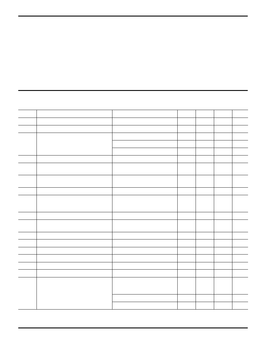
ELECTRICAL CHARACTERISTICS
Unless otherwise specified, V
CC
= 5V ±10%, T
A
= Operating Temperature Range (Note 1)
SYMBOL
PARAMETER
CONDITIONS
MIN
TYP
MAX
UNITS
I
CC
Supply Current
No Load (V
CC
= 5V)
90
mA
A
V
Low Frequency Gain (All Channels)
V
IN
= 100mV
P-P
at 300kHz
5.34
6.0
6.65
dB
V
SYNC
Channel Sync Output Level
CV/Y, R/Y, G/Y
Sync Present and Clamp Settled
0.6
0.9
1.1
V
B/C
Sync Present and Clamp Settled
1.2
1.4
1.5
V
Unfiltered
Sync Present and Clamp Settled
0.7
1.0
1.2
V
t
CLAMP
Clamp Response Time
Settled to Within 10mV, C
IN
=0.1µF
10
ms
f
0.5dB
0.5dB Bandwidth
All Outputs
4.5
MHz
(Flatness. All Filtered Channels)
f
C
3dB Bandwidth
All Outputs (With no Peaking Cap.
6.7
7.1
MHz
(Flatness. All Filtered Channels)
See Figures 2 and 13)
0.8f
C
0.8 x f
C
Attenuation, All Filtered Channels
All Outputs
1.5
dB
f
SB
Stopband Rejection
All Filtered Channels
35
41
dB
f
IN
= 27MHz to 100MHz worst case
(See Figures 2 and 13)
V
i
Input Signal Dynamic Range (All Channels) AC Coupled
1
1.25
V
P-P
NOISE
Output Noise (All Channels)
Over a Frequency Band
1
mV
RMS
of 25Hz-50MHz
OS
Peak Overshoot (All Channels)
2V
P-P
Output Pulse
4.3
%
I
SC
Output Short Circuit Current (All Channels) Note 2
120
mA
C
L
Output Load Capacitance (All Channels)
Load at the Output Pin
35
pF
dG
Differential Gain (All Channels)
All Outputs
0.4
%
d
F
Differential Phase (All Channels)
All Outputs
0.4
º
T
HD
Output Distortion (All Channels)
V
OUT
= 1.8V
P-P
at 3.58/4.43MHz
0.4
%
X
TALK
Crosstalk
Input of 0.5V
P-P
at 3.58/4.43MHz
55
dB
on any channel to output of any
other channel
Input A/
B
MUX Crosstalk
Input of 0.5V
P-P
at 3.58/4.43MHz
54
dB
Swap Mux Crosstalk
Input of 0.5V
P-P
at 3.58/4.43MHz
52
dB
ABSOLUTE MAXIMUM RATINGS
Absolute maximum ratings are those values beyond which
the device could be permanently damaged. Absolute
maximum ratings are stress ratings only and functional
device operation is not implied.
V
CC ..................................................................................................
6V
Junction Temperature ............................................. 150°C
ESD ..................................................................... >2000V
Storage Temperature Range...................... 65°C to 150°C
Lead Temperature (Soldering, 10 sec) ..................... 260°C
Thermal Resistance (
q
JA
) ...................................... 80°C/W
OPERATING CONDITIONS
Temperature Range ........................................ 0°C to 70°C
V
DD
Range ................................................... 4.5V to 5.5V
ML6427
5
Note 1:
Limits are guaranteed by 100% testing, sampling, or correlation with worst case test conditions.
Note 2:
Sustained short circuit protection limited to 10 seconds.
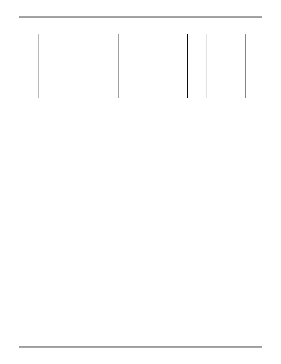
ELECTRICAL CHARACTERISTICS
(Continued)
SYMBOL
PARAMETER
CONDITIONS
MIN
TYP
MAX
UNITS
PSRR
PSRR (All Channels)
0.5V
P-P
(100kHz) at V
CC
39
dB
t
pd
Group Delay (All Channels)
at 100kHz
60
ns
Dt
pd
Group Delay Deviation from Flatness
to 3.58MHz (NTSC)
4
ns
to 4.43MHz (PAL)
7
ns
(All Channels)
to 10MHz
12
ns
V
IH
Input Voltage Logic High
A/
B
MUX, SWAP CVU, SWAP CVF
2.5
V
V
IL
Input Voltage Logic Low
A/
B
MUX, SWAP CVU, SWAP CVF
1
V