 | ÐлекÑÑоннÑй компоненÑ: ML6553 | СкаÑаÑÑ:  PDF PDF  ZIP ZIP |
Äîêóìåíòàöèÿ è îïèñàíèÿ www.docs.chipfind.ru
www.fairchildsemi.com
REV. 1.0.2 3/21/01
Features
· Can source and sink up to 1A
· Generates termination voltages for DDR SDRAM,
SSTL_2 SDRAM, SGRAM, or equivalent memories
· Generates termination voltages for active termination
schemes for GTL+, DDR, Rambus
TM
, VME, LV-TTL,
PECL and other high speed logic
· V
L
regulated to within 3% at 800mA
· Minimum external components. Requires no feedback
compensation
· Fixed frequency operation for easier system integration
· Lower power consumption than passive, resistor divider
termination, reducing heat by as much as 50%
· Separate voltages for V
CCQ
and PV
DD
General Description
The ML6553 switching regulator is designed to convert
voltage supplies ranging from 2.0V to 3.6V into a desired
output voltage or termination voltage for various applica-
tions. The ML6553 can be implemented to produce
regulated output voltages in two different modes. In the
default mode, the output is 50% of voltage applied to V
CCQ
.
The switching regulator is capable of sourcing or sinking up
to 1A of current.
The ML6553, used in conjunction with series termination
resistors, provides an excellent voltage source for active
termination schemes of high speed transmission lines as
those seen in high speed memory buses and distributed back-
plane designs. The voltage output of the regulator can be
used as a termination voltage for other bus interface
standards such as SSTL, DDR, Rambus
TM
, GTL+, VME,
LV-CMOS, LV-TTL, P-ECL, and CMOS.
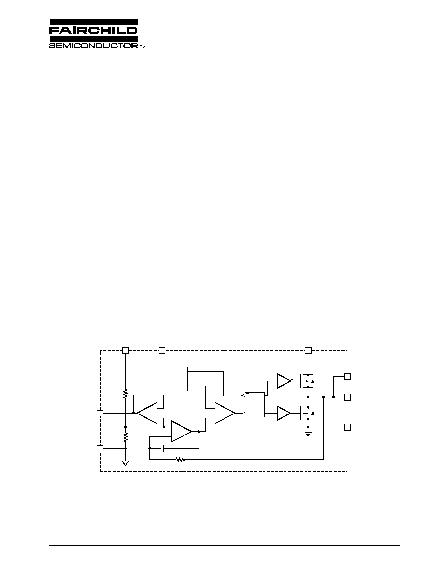
Block Diagram
VL
AGND
190k
BUFFER
3
VCCQ/2
7
AVCC
CLK
RAMP
VINTEG
PWM
COMPARATOR
4
PVDD
Q1
Q2
5
8
DGND
VL
6
+
+
+
VCCQ
1
OSCILLATOR/
RAMP GENERATOR
S
R
Q
Q
2
190k
ML6553
Bus Termination Regulator
ML6553
PRODUCT SPECIFICATION
2
REV. 1.0.2 3/21/01
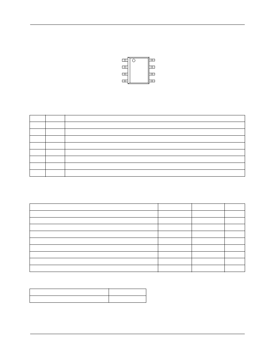
Pin Configuration
Pin Description
Absolute Maximum Ratings
Absolute maximum ratings are those values beyond which the device could be permanently damaged. Absolute maximum
ratings are stress ratings only and functional device operation is not implied.
Operating Conditions
Pin Name
Function
1
V
CCQ
Voltage supply for internal reference voltage divider
2
V
CCQ/2
V
REF
output is V
CCQ/2
3
AGND
Analog signal ground
4
AV
CC
Voltage supply for the noise sensitive analog control section.
5
PV
DD
Voltage supply for the internal power transistors.
6
V
L
Output inductor connection
7
V
L
Output inductor connection
8
DGND
Return for the internal power transistors.
Parameter
Min.
Max.
Unit
V
IN
5
V
Voltage on Any Other Pin
GND 0.3
V
IN
+ 0.3
V
Peak Switch Current (I
PEAK
)
1
A
Average Switch Current (I
AVG
)
300
mA
Junction Temperature
150
°C
Storage Temperature Range
65
150
°C
Lead Temperature (Soldering, 10 sec)
150
°C
Thermal Resistance (
JA
)
160
°C/W
Output Current, Source or Sink
1
A
Temperature Range
0°C to 70°C
AV
CC
, PV
DD
Operating Range
2.0V to 3.6V
ML6553
8-Pin SOIC (S08)
1
2
3
4
8
7
6
5
VCCQ
VCCQ/2
AGND
AVCC
DGND
VL
VL
PVDD
TOP VIEW
PRODUCT SPECIFICATION
ML6553
REV. 1.0.2 3/21/01
3
Electrical Characteristics
AV
CC
= PV
DD
= 3.3V ±10%. Unless otherwise specified, T
A
= Operating Temperature Range (Note 1)
Notes:
1. Limits are guaranteed by 100% testing, sampling, or correlation with worst-case test conditions.
2. Specifications are taken from the application circuit in Figure 2 using the recommended component values.
Symbol
Parameter
Conditions
Min
Typ
Max Units
Switching Regulator
V
TT
Output Voltage, V
TT
I
OUT
= 0,
V
CCQ
= 2.3V
1.12
1.15
1.18
V
(See Figure 2)
V
REF
= open
V
CCQ
= 2.5V
1.22
1.25
1.28
V
V
CCQ
= 2.7V
1.32
1.35
1.38
V
I
OUT
= ±1A,
V
CCQ
= 2.3V
1.09
1.15
1.21
V
V
REF
= open
V
CCQ
= 2.5V
1.19
1.25
1.31
V
Note 2
V
CCQ
= 2.7V
1.28
1.35
1.42
V
V
CCQ/2
Output Voltage, V
CCQ/2
V
CCQ
= 2.3V 1.139 1.15 1.162
V
V
CCQ
= 2.5V 1.238
1.25
1.263
V
V
CCQ
= 2.7V 1.337 1.35 1.364
V
Source Resistance from V
L
20
m
Switching Frequency
650
kHz
I
REF
Output Load Current for V
CCQ/2
Pin
3
mA
Supply
I
Q
Quiescent Current
I
OUT
= 0, no load
I
VCCQ
10
µA
I
AVCC
500
µA
IPV
DD
4.5
mA
ML6553
PRODUCT SPECIFICATION
4
REV. 1.0.2 3/21/01
Functional Description
The ML6553 switching regulator is designed to sink and
source 1A load current and maintain a tight output voltage
regulation without the need for external feedback. Feedback
is accomplished internally by setting the average value of V
L
equal to V
CCQ/2
through a high gain error amp. The
ML6553 implements an open loop design that does not
require external loop compensation, providing a simplified
regulator design that can be used in cost sensitive applica-
tions.
Regulator Operation
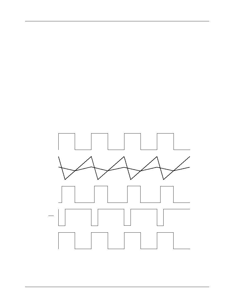
Refer to the block diagram on the first page of this datasheet.
The oscillator/ramp block generates a 650kHz clock pulse
that is used to set the flip-flop. It also generates a 650kHz
ramp that the PWM comparator uses to reset the flip-flop.
When the flip-flop is set, the high side switch (Q1) is turned
on and the low side switch (Q2) is held off. In this state, the
voltage at V
L
is pulled up to PV
DD
, which the error amp,
integrates and inverts. The resulting output voltage of the
error amp will decline until it intersects the rising voltage of
the ramp. When this occurs the flip-flop is reset. In the reset
state, the high side switch is off, the low side switch is on
and V
L
is pulled to DGND. The flip-flop will remain in the
reset state until the next clock pulse. A timing diagram is
shown in Figure 1.
In the absence of a load, the duty cycle will be 50% if the
PV
DD
and V
CCQ
are the same. The average voltage at V
L
will be half the voltage applied to V
CCQ
, and the net current
change will be zero. If the ML6553 needs to source current,
the duty cycle will increase, resulting in more current being
supplied to the load. If the ML6553 needs to sink current, the
duty will decrease, resulting in current being pulled from the
load and returned back to the PV
DD
supply.
Figure 1. Timing Diagram
VL
Q
PWMCMP
RAMP
VINTEG
CLK
PRODUCT SPECIFICATION
ML6553
REV. 1.0.2 3/21/01
5
Design Consideration
Inductor Selection
The ML6553 requires the selection of an external inductor.
A value of 4.7µH is a good choice, but any value between
2.2µH and 10µH is acceptable. Choosing an inductance
value of less than 2.2µH will reduce the component's foot-
print or the DC resistance, but the output voltage ripple will
increase. Conversely, inductance values greater than 10µH
will reduce the output ripple, but component size and output
regulation become issues.
It is important to use an inductor that is rated to handle 1.5A
peak currents without saturating. Also look for an inductor
with low winding resistance. An inductor with low winding
resistance leads to better regulation and higher output current
capability. A good rule of thumb is to use inductors with
20m
or less of winding resistance.
The final selection of the inductor will be based on trade-offs
between size, cost and performance. Make your selections
carefully. Inductor tolerance, core and copper loss will vary
with the type of inductor selected and should be evaluated
with the ML6553 under worst case conditions to determine
its suitability.
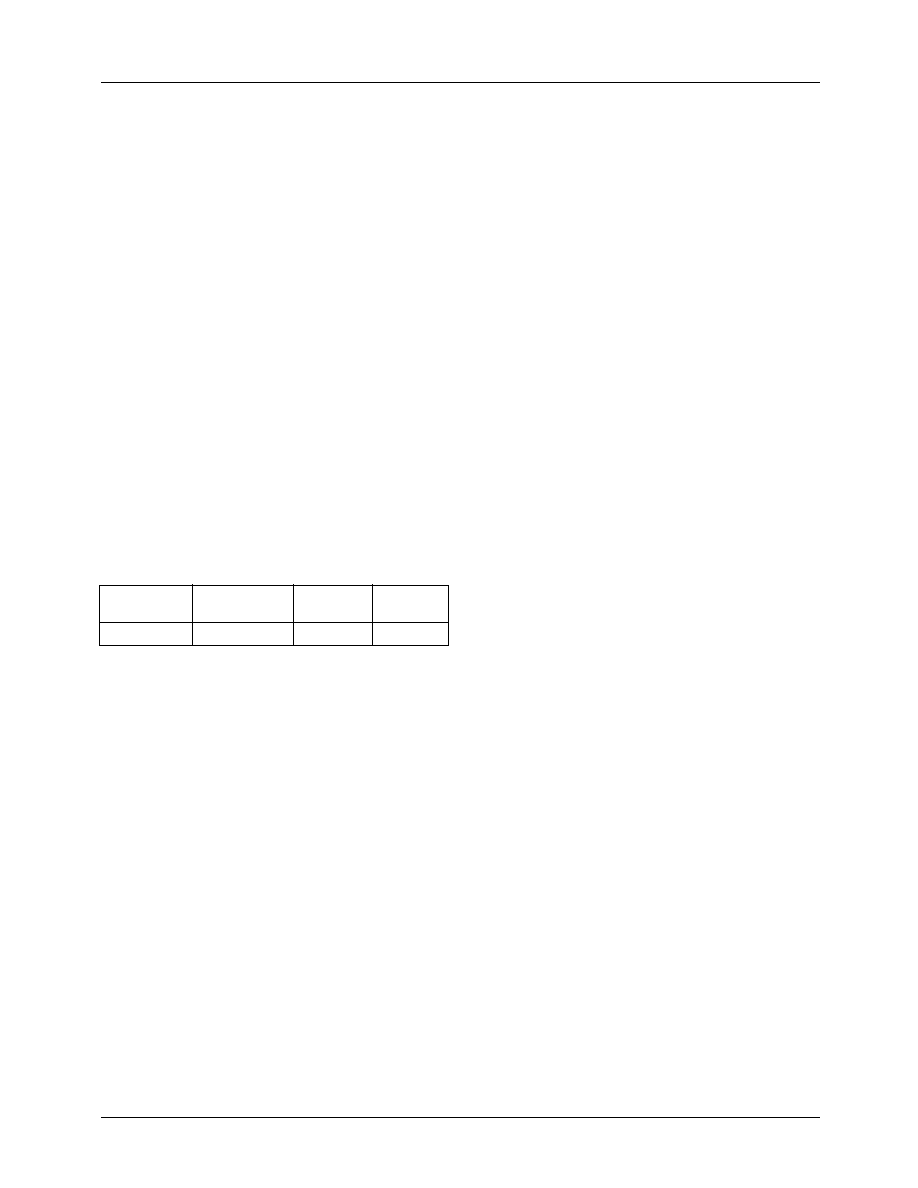
Suggested inductor for L1:
Coiltronics
(561) 241-7876
Output Capacitor
The output capacitor filters the pulses of current from the bus
terminator regulator as well as lowers the AC output imped-
ance. For the best performance, one 330µF OS-CON decou-
pling capacitor is recommended.
Note that data transitions on the bus cause fast changes in
output current. These fast current changes cause high
frequency spikes to appear on the output. To minimize these
effects, choose an output capacitor with a combined ESR of
less than 50m
and use good layout practices to minimize
trace inductance from the output capacitors to the termina-
tion resistors. In addition, it is also recommended to bypass
the termination resistors with 0.01µF ceramic capacitors.
Suitable capacitors can be obtained from the following
vendors:
AVX
(207) 282-5111
TPS Series
Sanyo
(619) 661-6835
OS-CON Series
Input Capacitor
It is recommended to de-couple the PV
DD
input with a 47µF
to 100µF capacitor. This provides the benefits of preventing
the input ripple from affecting the ML6553 control circuitry,
as well as improves the efficiency by reducing the I squared
R losses during the charge cycle of the inductor. Again, a low
ESR capacitor (such as tantalum) is recommended.
The AV
CC
input should be de-coupled with at least a
ceramic capacitor but a low pass RC filter is recommended if
the supply is particularly noisy. If a RC filter is used, the
series resistor value needs to low enough to prevent exces-
sive voltage drops and high enough to provide effective
filtering. Resistor values on the order of 100
are accept-
able.
The V
CCQ
pin can also be bypassed with a ceramic capacitor
if noise is present. The V
CCQ
pin can be de-coupled with a
low pass RC filter if there is significant noise pickup on its
input. If a RC filter is used, resistor values on the order of
1,000
are acceptable.
Layout
Good layout practices will ensure the proper operation of the
ML6553. Some layout guidelines follow:
· Use adequate ground and power traces or planes.
· Keep the 47µF-100µF input capacitor as close to PV
DD
and DGND as possible.
· Use short trace lengths from the inductor to the V
L
pins
and from the inductor to the output capacitors.
· Use a separate trace from AGND to DGND, and use
DGND as the ground point for all the power components.
· Use additional bypass capacitors at each termination
resistor pack.
A typical application circuit schematic is shown in Figure 2,
and a sample layout is shown in Figure 3.
Where L
DCR
is the DC resistance of the output inductor, L1
in Figure 2, and 0.020 is the source resistance of the output
V
L
. Both L
DCR
and 0.020 are in Ohms.
Manufacturer
Part No.
Inductance
DC
Resistance
Coiltronics
UP3-4R7
4.7µH
0.011
I
OUT MAX
(
)
DESIRED
OVA
OUTPUT
OVA
(
) V
TT
×
L
DCR
0.020
+
--------------------------------------------------------------------------------------------------------
=
(1)