October 1987
Revised January 1999
MM74C154 4-Li
ne to 16-
Line Decoder
/Dem
ult
i
pl
e
x
e
r
© 1999 Fairchild Semiconductor Corporation
DS005893.prf
www.fairchildsemi.com
MM74C154
4-Line to 16-Line Decoder/Demultiplexer
General Description
The MM74C154 one of sixteen decoder is a monolithic
complementary MOS (CMOS) integrated circuit con-
structed with N- and P-channel enhancement transistors.
The device is provided with two strobe inputs, both of
which must be in the logical "0" state for normal operation.
If either strobe input is in the logical "1" state, all 16 outputs
will go to the logical "1" state.
To use the product as a demultiplexer, one of the strobe
inputs serves as a data input terminal, while the other
strobe input must be maintained in the logical "0" state. The
information will then be transmitted to the selected output
as determined by the 4-line input address.
Features
s
Supply voltage range:
3V to 15V
s
Tenth power TTL compatible:
Drive 2 LPTTL loads
s
High noise margin:
1V guaranteed
s
High noise immunity:
0.45 V
CC
(typ.)
Applications
∑ Automotive
∑ Data terminals
∑ Instrumentation
∑ Medical electronics
∑ Alarm systems
∑ Industrial electronics
∑ Remote metering
∑ Computers
Ordering Code:
Devices also available in Tape and Reel. Specify by appending the suffix letter "X" to the ordering code.
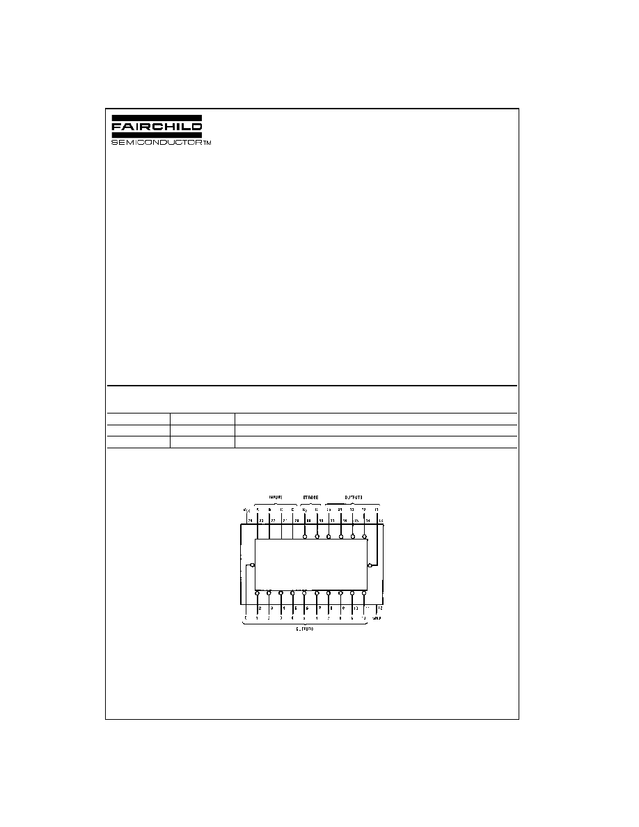
Connection Diagram
Pin Assignments for DIP and SOIC
Top View
Order Number
Package Number
Package Description
MM74C154WM
M24B
24-Lead Small Outline Integrated Circuit (SOIC), JEDEC MS-013, 0.300" Wide
MM74C154N
N24A
24-Lead Plastic Dual-In-Line Package (PDIP), JEDEC MS-010, 0.600" Wide
www.fairchildsemi.com
2
M
M
74C154
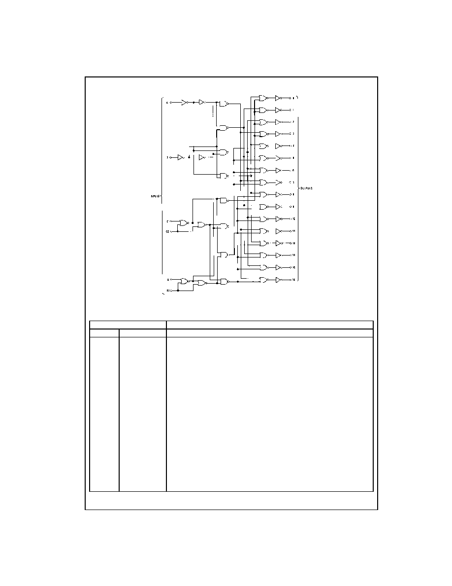
Logic Diagram
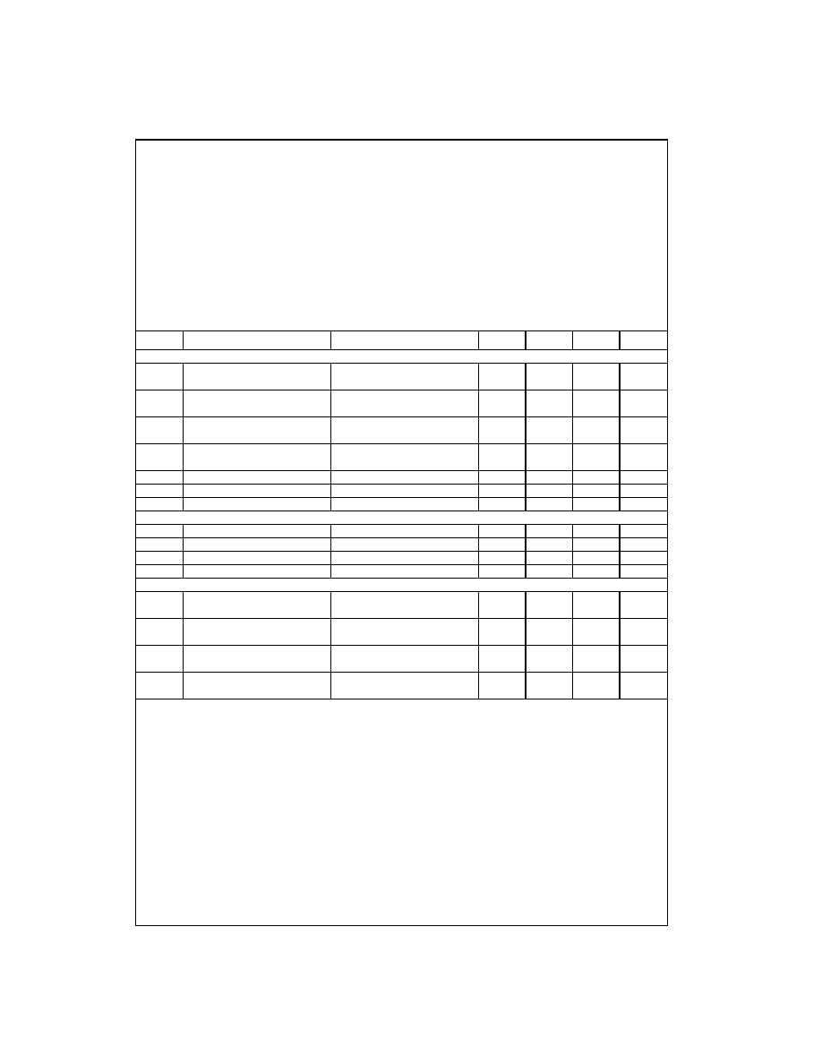
Truth Table
X
=
"Don't Care" Condition
Inputs
Outputs
G1
G2
D
C
B
A
0
1
2
3
4
5
6
7
8
9
10
11
12
13
14
15
L
L
L
L
L
L
L
H
H
H
H
H
H
H
H
H
H
H
H
H
H
H
L
L
L
L
L
H
H
L
H
H
H
H
H
H
H
H
H
H
H
H
H
H
L
L
L
L
H
L
H
H
L
H
H
H
H
H
H
H
H
H
H
H
H
H
L
L
L
L
H
H
H
H
H
L
H
H
H
H
H
H
H
H
H
H
H
H
L
L
L
H
L
L
H
H
H
H
L
H
H
H
H
H
H
H
H
H
H
H
L
L
L
H
L
H
H
H
H
H
H
L
H
H
H
H
H
H
H
H
H
H
L
L
L
H
H
L
H
H
H
H
H
H
L
H
H
H
H
H
H
H
H
H
L
L
L
H
H
H
H
H
H
H
H
H
H
L
H
H
H
H
H
H
H
H
L
L
H
L
L
L
H
H
H
H
H
H
H
H
L
H
H
H
H
H
H
H
L
L
H
L
L
H
H
H
H
H
H
H
H
H
H
L
H
H
H
H
H
H
L
L
H
L
H
L
H
H
H
H
H
H
H
H
H
H
L
H
H
H
H
H
L
L
H
L
H
H
H
H
H
H
H
H
H
H
H
H
H
L
H
H
H
H
L
L
H
H
L
L
H
H
H
H
H
H
H
H
H
H
H
H
L
H
H
H
L
L
H
H
L
H
H
H
H
H
H
H
H
H
H
H
H
H
H
L
H
H
L
L
H
H
H
L
H
H
H
H
H
H
H
H
H
H
H
H
H
H
L
H
L
L
H
H
H
H
H
H
H
H
H
H
H
H
H
H
H
H
H
H
H
L
L
H
X
X
X
X
H
H
H
H
H
H
H
H
H
H
H
H
H
H
H
H
H
L
X
X
X
X
H
H
H
H
H
H
H
H
H
H
H
H
H
H
H
H
H
H
X
X
X
X
H
H
H
H
H
H
H
H
H
H
H
H
H
H
H
H
3
www.fairchildsemi.com
MM74C154
Absolute Maximum Ratings
(Note 1)
Note 1: "Absolute Maximum Ratings" are those values beyond which the
safety of the device cannot be guaranteed. Except for "Operating Tempera-
ture Range" they are not meant to imply that the devices should be oper-
ated at these limits. The table of "Electrical Characteristics" provides
conditions for actual device operation.
DC Electrical Characteristics
Min/max limits apply across temperature range unless otherwise noted
Voltage at Any Pin
-
0.3V to V
CC
+
0.3V
Operating Temperature Range
-
40
∞
C to
+
85
∞
C
Storage Temperature Range
-
65
∞
C to
+
150
∞
C
Maximum V
CC
Voltage
18V
Power Dissipation
Dual-In-Line
700 mW
Small Outline
500 mW
Operating V
CC
Range
3V to 15V
Lead Temperature
(Soldering, 10 seconds)
260
∞
C
Symbol
Parameter
Conditions
Min
Typ
Max
Units
CMOS TO CMOS
V
IN(1)
Logical "1" Input Voltage
V
CC
=
5.0V
3.5
V
V
CC
=
10V
8.0
V
V
IN(0)
Logical "0" Input Voltage
V
CC
=
5.0V
1.5
V
V
CC
=
10V
2.0
V
V
OUT(1)
Logical "1" Output Voltage
V
CC
=
5.0V, I
O
=
-
10
µ
A
4.5
V
V
CC
=
10V, I
O
=
-
10
µ
A
9.0
V
V
OUT(0)
Logical "0" Output Voltage
V
CC
=
5.0V, I
O
=
10
µ
A
0.5
V
V
CC
=
10V, I
O
=
10
µ
A
1.0
V
I
IN(1)
Logical "1" Input Current
V
CC
=
15V, V
IN
=
15V
0.005
1.0
µ
A
I
IN(0)
Logical "0" Input Current
V
CC
=
15V, V
IN
=
0V
-
1.0
-
0.005
µ
A
I
CC
Supply Current
V
CC
=
15V
0.05
300
µ
A
CMOS TO LPTTL INTERFACE
V
IN(1)
Logical "1" Input Voltage
V
CC
=
4.75V
V
CC
-
1.5
V
V
IN(0)
Logical "0" Input Voltage
V
CC
=
4.75V
0.8
V
V
OUT(1)
Logical "1" Output Voltage
V
CC
=
4.75V, I
O
=
-
100
µ
A
2.4
V
V
OUT(0)
Logical "0" Output Voltage
V
CC
=
4.75V, I
O
=
360
µ
A
0.4
V
OUTPUT DRIVE (See Family Characteristics Data Sheet) (Short Circuit Current)
I
SOURCE
Output Source Current
V
CC
=
5.0V, V
IN(0)
=
0V
-
1.75
mA
T
A
=
25
∞
C, V
OUT
=
0V
I
SOURCE
Output Source Current
V
CC
=
10V, V
IN(0)
=
0V
-
8.0
mA
T
A
=
25
∞
C, V
OUT
=
0V
I
SINK
Output Sink Current
V
CC
=
5.0V, V
IN(1)
=
5.0V
1.75
mA
T
A
=
25
∞
C, V
OUT
=
V
CC
I
SINK
Output Sink Current
V
CC
=
10V, V
IN(1)
=
10V
8.0
mA
T
A
=
25
∞
C, V
OUT
=
V
CC
www.fairchildsemi.com
4
M
M
74C154
AC Electrical Characteristics
(Note 2)
T
A
=
25
∞
C, C
L
=
50 pF, unless otherwise noted
Note 2: AC Parameters are guaranteed by DC correlated testing.
Note 3: Capacitance is guaranteed by periodic testing.
Note 4: C
PD
determines the no load AC power consumption of any CMOS device. For complete explanation see Family Characteristics Application Note
AN-90.
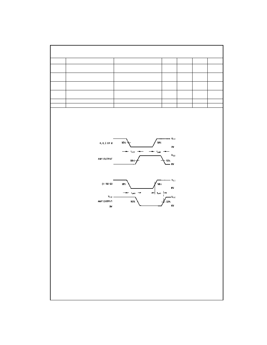
Switching Time Waveforms
t
r
=
t
f
=
20 ns
Symbol
Parameter
Conditions
Min
Typ
Max
Units
t
pd0
Propagation Delay to a Logical
V
CC
=
5.0V
275
400
ns
"0" from Any Input to Any Output
V
CC
=
10V
100
200
ns
t
pd0
Propagation Delay to a Logical
V
CC
=
5.0V
275
400
ns
"0" from G1 or G2 to Any Output
V
CC
=
10V
100
200
ns
t
pd0
Propagation Delay to a Logical
V
CC
=
5.0V
265
400
ns
"0" from Any Input to Any Output
V
CC
=
10V
100
200
ns
t
pd1
Propagation Delay to a Logical
V
CC
=
5.0V
265
400
ns
"1" from G1 or G2 to Any Output
V
CC
=
10V
100
200
ns
C
IN
Input Capacitance
(Note 3)
5.0
pF
C
PD
Power Dissipation Capacitance
(Note 4)
60
pF
5
www.fairchildsemi.com
MM74C154
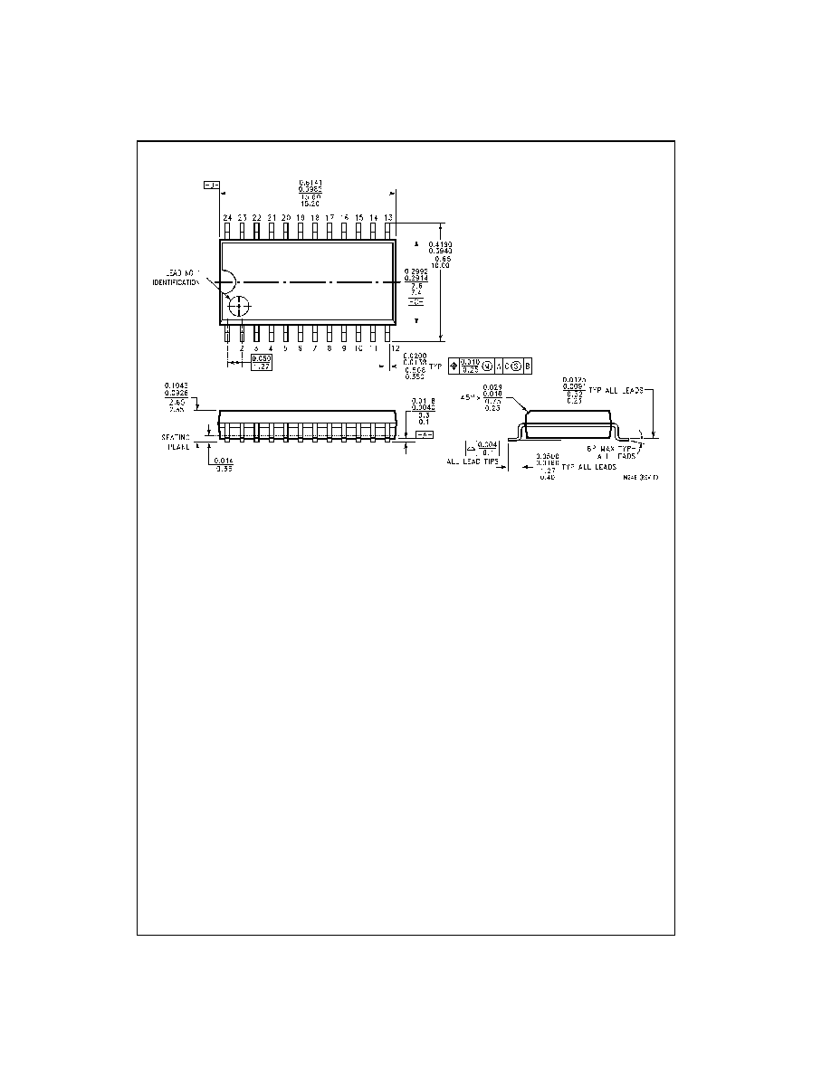
Physical Dimensions
inches (millimeters) unless otherwise noted
24-Lead Small Outline Integrated Circuit (SOIC), JEDEC MS-013, 0.300" Wide
Package Number M24B