 | –≠–ª–µ–∫—Ç—Ä–æ–Ω–Ω—ã–π –∫–æ–º–ø–æ–Ω–µ–Ω—Ç: MM74C164 | –°–∫–∞—á–∞—Ç—å:  PDF PDF  ZIP ZIP |
October 1987
Revised January 1999
MM74C164 8-Bi
t P
a
ral
l
el
-Out
Ser
i
al
Shi
f
t
R
e
gist
er
© 1999 Fairchild Semiconductor Corporation
DS005896.prf
www.fairchildsemi.com
MM74C164
8-Bit Parallel-Out Serial Shift Register
General Description
The MM74C164 shift registers are a monolithic comple-
mentary MOS (CMOS) integrated circuit constructed with
N- and P-channel enhancement transistors. These 8-bit
shift registers have gated serial inputs and clear. Each reg-
ister bit is a D-type master/slave flip-flop. A high-level input
enables the other input which will then determine the state
of the flip-flop.
Data is serially shifted in and out of the 8-bit register during
the positive going transition of clock pulse. Clear is inde-
pendent of the clock and accomplished by a low level at the
clear input. All inputs are protected against electrostatic
effects.
Features
s
Supply voltage range:
3V to 15V
s
Tenth power TTL compatible:
drive 2 LPTTL loads
s
High noise immunity:
0.45 V
CC
(typ.)
s
Low power:
50 nW (typ.)
s
Medium speed operation:
0.8 MHz (typ.) with 10V
supply
Applications
∑ Data terminals
∑ Instrumentation
∑ Medical electronics
∑ Alarm systems
∑ Industrial electronics
∑ Remote metering
∑ Computers
Ordering Code:
Devices also available in Tape and Reel. Specify by appending the suffix letter "X" to the ordering code.
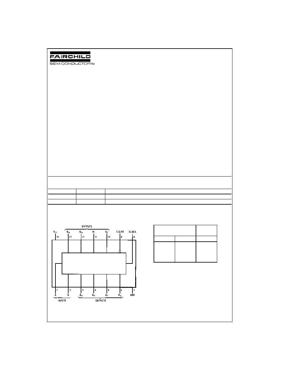
Connection Diagram
Pin Assignments for DIP and SOIC
Top View
Truth Table
Serial Inputs A and B
Order Number
Package Number
Package Description
MM74C164M
M14A
14-Lead Small Outline Integrated Circuit (SOIC), JEDEC MS-120, 0.150" Narrow
MM74C164N
N14A
14-Lead Plastic Dual-In-Line (PDIP), JEDEC MS-001, 0.300" Wide
Inputs
Output
t
n
t
n
+
1
A
B
Q
A
1
1
1
0
1
0
1
0
0
0
0
0
www.fairchildsemi.com
2
M
M
74C164
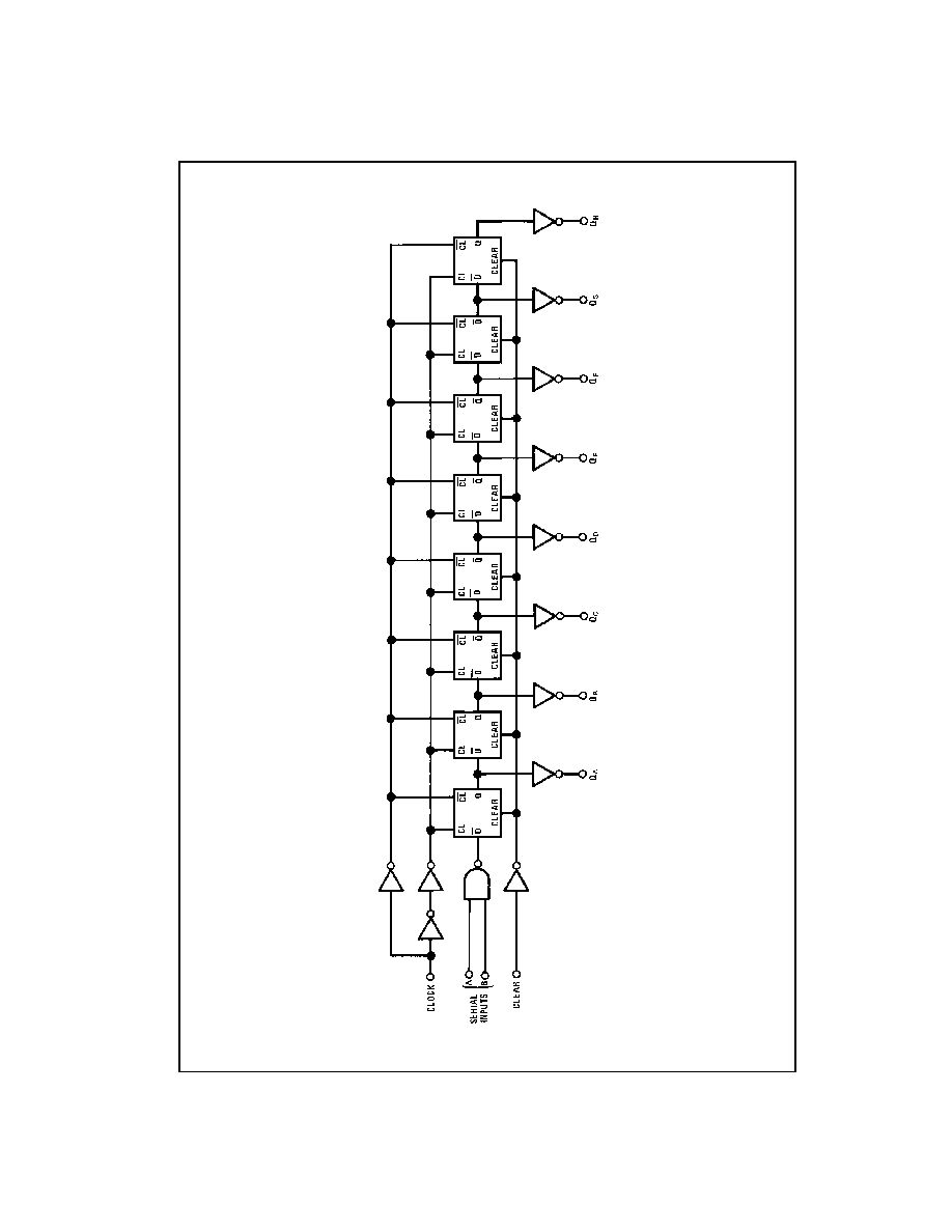
Block Diagram
3
www.fairchildsemi.com
MM74C164
Absolute Maximum Ratings
(Note 1)
Note 1: "Absolute Maximum Ratings" are those values beyond which the
safety of the device cannot be guaranteed. Except for "Operating Tempera-
ture Range" they are not meant to imply that the devices should be oper-
ated at these limits. The table of "Electrical Characteristics" provides
conditions for actual device operation.
DC Electrical Characteristics
Min/Max limits apply across temperature range unless otherwise noted
Voltage at Any Pin
-
0.3V to V
CC
+
0.3V
Operating Temperature Range
-
40
∞
C to
+
85
∞
C
Storage Temperature Range
-
65
∞
C to
+
150
∞
C
Absolute Maximum V
CC
18V
Power Dissipation (P
D
)
Dual-In-Line
700 mW
Small Outline
500 mW
Operating V
CC
Range
3V to 15V
Lead Temperature
(soldering, 10 seconds)
260
∞
C
Symbol
Parameter
Conditions
Min
Typ
Max
Units
CMOS TO CMOS
V
IN(1)
Logical "1" Input Voltage
V
CC
=
5V
3.5
V
V
CC
=
10V
8.0
V
V
IN(0)
Logical "0" Input Voltage
V
CC
=
5V
1.5
V
V
CC
=
10V
2.0
V
V
OUT(1)
Logical "1" Output Voltage
V
CC
=
5V, I
O
=
-
10
µ
A
4.5
V
V
CC
=
10V, I
O
=
-
10
µ
A
9.0
V
V
OUT(0)
Logical "0" Output Voltage
V
CC
=
5V, I
O
=
+
10
µ
A
0.5
V
V
CC
=
10V, I
O
=
+
10
µ
A
1.0
V
I
IN(1)
Logical "1" Input Current
V
CC
=
15V, V
IN
=
15V
0.005
1.0
µ
A
I
IN(0)
Logical "0" Input Current
V
CC
=
15V, V
IN
=
0V
-
1.0
-
0.005
µ
A
I
CC
Supply Current
V
CC
=
15V
0.05
300
µ
A
CMOS TO LPTTL INTERFACE
V
IN(1)
Logical "1" Input Voltage
V
CC
=
4.75V
V
CC
-
1.5
V
V
IN(0)
Logical "0" Input Voltage
V
CC
=
4.75V
0.8
V
V
OUT(1)
Logical "1" Output Voltage
V
CC
=
4.75V, I
O
=
-
360
µ
A
2.4
V
V
OUT(0)
Logical "0" Output Voltage
V
CC
=
4.75V, I
O
=
360
µ
A
0.4
V
OUTPUT DRIVE (See Family Characteristics Data Sheet) (Short Circuit Current)
I
SOURCE
Output Source Current
V
CC
=
5V, V
IN(0)
=
0V
-
1.75
mA
T
A
=
25
∞
C, V
OUT
=
0V
I
SOURCE
Output Source Current
V
CC
=
10V, V
IN(0)
=
0V
-
8.0
mA
T
A
=
25
∞
C, V
OUT
=
0V
I
SINK
Output Sink Current
V
CC
=
5V, V
IN(1)
=
5V
1.75
mA
T
A
=
25
∞
C, V
OUT
=
V
CC
I
SINK
Output Sink Current
V
CC
=
10V, V
IN(1)
=
10V
8.0
mA
T
A
=
25
∞
C, V
OUT
=
V
CC
www.fairchildsemi.com
4
M
M
74C164
AC Electrical Characteristics
(Note 2)
T
A
=
25
∞
C, C
L
=
50 pF, unless otherwise noted
Note 2: AC Parameters are guaranteed by DC correlated testing.
Note 3: Capacitance is guaranteed by periodic testing.
Note 4: C
PD
determines the no load AC power consumption of any CMOS device. For complete explanation see Family Characteristics application note
AN-90.
Typical Applications
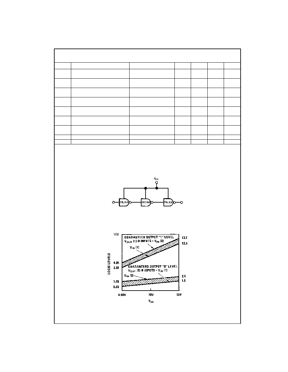
74C Compatibility
Guaranteed Noise Margin
as a Function of V
CC
Symbol
Parameter
Conditions
Min
Typ
Max
Units
t
pd1
Propagation Delay Time to a Logical "0" or a
V
CC
=
5V
230
310
ns
Logical "1" from Clock to Q
V
CC
=
10V
90
120
ns
t
pd0
Propagation Delay Time to a Logical "0" from V
CC
=
5V
280
380
ns
Clear to Q
V
CC
=
10V
110
150
ns
t
S
Time Prior to Clock Pulse that Data
V
CC
=
5V
200
110
ns
Must be Present
V
CC
=
10V
80
30
ns
t
H
Time After Clock Pulse that
V
CC
=
5V
0
0
ns
Data Must be Held
V
CC
=
10V
0
0
ns
f
MAX
Maximum Clock Frequency
V
CC
=
5V
2.0
3
MHz
V
CC
=
10V
5.5
8
MHz
t
W
Minimum Clear Pulse Width
V
CC
=
5V
150
250
ns
V
CC
=
10V
55
90
ns
t
r
, t
f
Maximum Clock Rise and Fall Time
V
CC
=
5V
15
µ
s
V
CC
=
10V
5
µ
s
C
IN
Input Capacitance
Any Input (Note 3)
5
pF
C
PD
Power Dissipation Capacitance
(Note 4)
140
pF
5
www.fairchildsemi.com
MM74C164
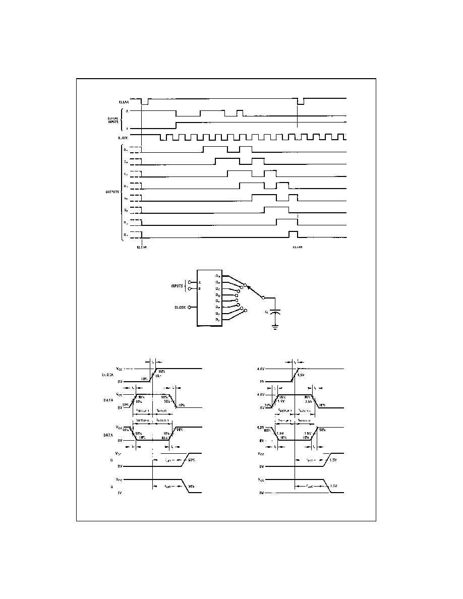
Logic Waveform
AC Test Circuit
Switching Time Waveforms
CMOS to CMOS
t
r
=
t
f
=
20 ns
TTL to CMOS