 | –≠–ª–µ–∫—Ç—Ä–æ–Ω–Ω—ã–π –∫–æ–º–ø–æ–Ω–µ–Ω—Ç: MM74C165 | –°–∫–∞—á–∞—Ç—å:  PDF PDF  ZIP ZIP |
October 1987
Revised January 1999
MM74C165
P
a
ral
l
el
-Loa
d 8-
Bit
Shi
f
t
Regi
st
er
© 1999 Fairchild Semiconductor Corporation
DS005897.prf
www.fairchildsemi.com
MM74C165
Parallel-Load 8-Bit Shift Register
General Description
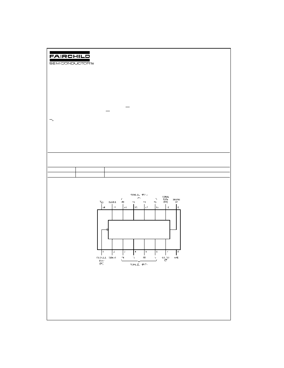
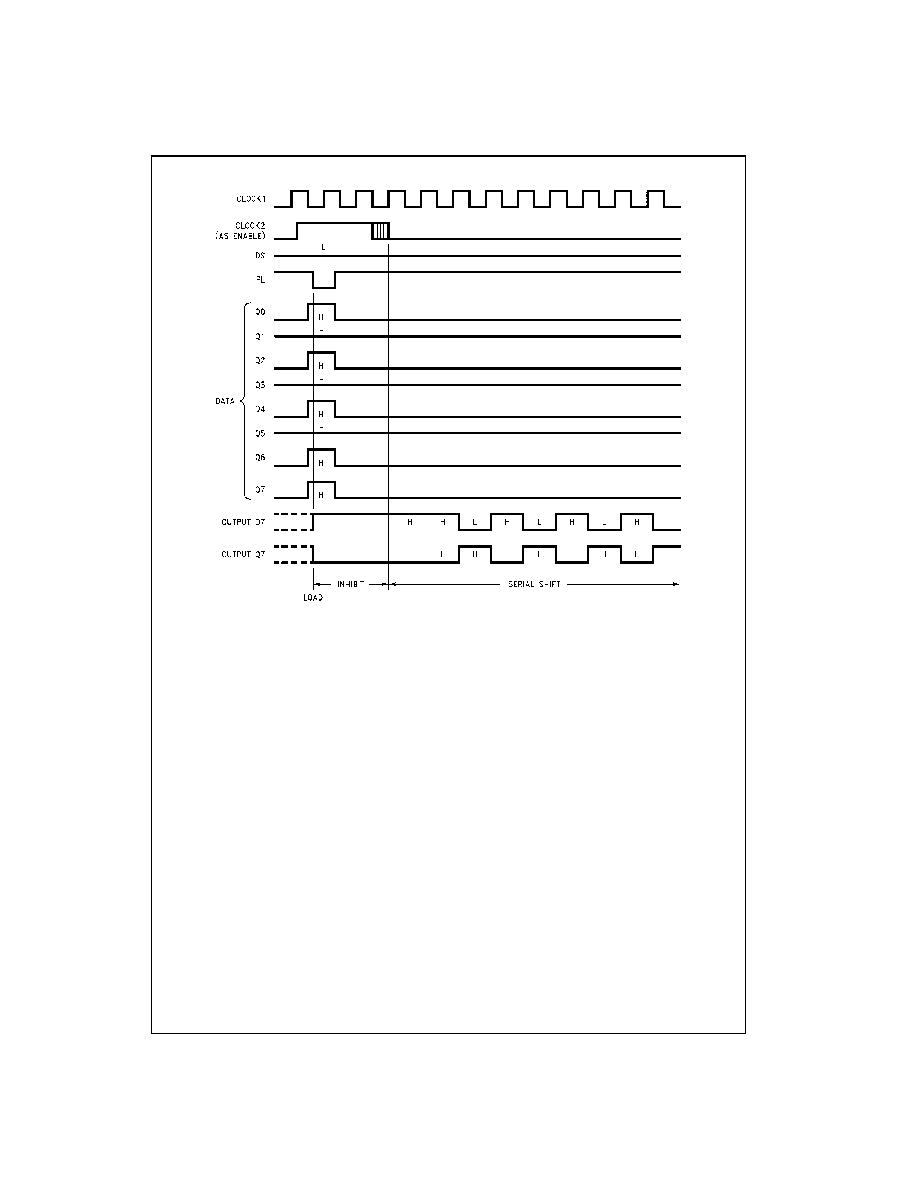
The MM74C165 functions as an 8-bit parallel-load, serial
shift register. Data is loaded into the register independent
of the state of the clock(s) when PARALLEL LOAD (PL) is
low. Shifting is inhibited as long as PL is low. Data is
sequentially shifted from complementary outputs, Q
7
and
Q
7
, highest-order bit (P7) first. New serial data may be
entered via the SERIAL DATA (Ds) input. Serial shifting
occurs on the rising edge of CLOCK1 or CLOCK2. Clock
inputs may be used separately or together for combined
clocking from independent sources. Either clock input may
be used also as an active-low clock enable. To prevent
double-clocking when a clock input is used as an enable,
the enable must be changed to a high level (disabled) only
while the clock is HIGH.
Features
s
Wide supply voltage range:
3V to 15V
s
Guaranteed noise margin:
1V
s
High noise immunity:
0.45 V
CC
(typ.)
s
Low power TTL compatibility:
fan out of 2 driving 74L
s
Parallel loading independent of clock
s
Dual clock inputs
s
Fully static operation
Ordering Code:
Connection Diagram
Pin Assignments for DIP
Top View
Order Number
Package Number
Package Description
MM74165N
N16E
16-Lead Plastic Dual-In-Line Package (PDIP), JEDEC MS-001, 0.300" Wide
www.fairchildsemi.com
2
M
M
74C165
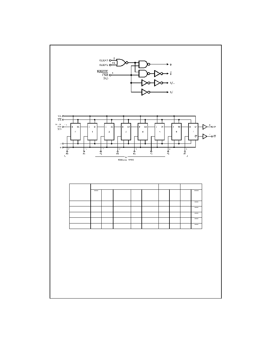
Block Diagrams
*Please look into Section 8, Appendix D for availability of various package types.
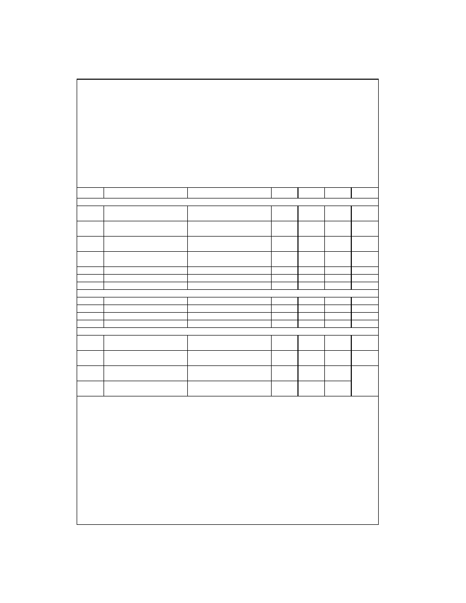
Truth Table
X
=
Don't Care
H
=
V
IN(1)
L
=
V
IN(0)
=
Clock transition from V
IN(0)
to V
IN(1)
P0 thru P7
=
Data present (and loaded into) parallel inputs
Q0 thru Q6
=
Internal flip-flop outputs
State
Inputs
Internal
Outputs
PL
Clock1
Clock2
Ds
P0 thru P7
Q0
Q1
Q7
Q7
(as enable)
Parallel Load
L
X
X
X
P0...P7
P0
P1
P7
P7
Enable
H
L
L
X
X
P0
P1
P7
P7
Shift (with Ds)
H
L
H
X
H
P0
P6
P6
Shift (with Ds)
H
L
L
X
L
H
P5
P5
Hold (Disable)
H
H
X
X
L
H
P5
P5
3
www.fairchildsemi.com
MM74C165
Absolute Maximum Ratings
(Note 1)
Note 1: "Absolute Maximum Ratings" are those values beyond which the
safety of the device cannot be guaranteed. Except for "Operating Tempera-
ture Range" they are not meant to imply that the devices should be oper-
ated at these limits. The Electrical Characteristics table provides conditions
for actual device operation.
DC Electrical Characteristics
Min/Max limits apply across temperature range unless otherwise noted
Voltage at Any Pin
-
0.3V to V
CC
+
0.3V
Operating Temperature Range
-
40
∞
C to
+
85
∞
C
Storage Temperature Range
-
65
∞
C to
+
150
∞
C
Absolute Maximum V
CC
18V
Power Dissipation
Dual-In-Line
700 mW
Small Outline
500 mW
Operating V
CC
Range
3V to 15V
Lead Temperature
(Soldering, 10 seconds)
260
∞
C
Symbol
Parameter
Conditions
Min
Typ
Max
Units
CMOS TO CMOS
V
IN(1)
Logical "1" Input Voltage
V
CC
=
5V
3.5
V
V
CC
=
10V
8.0
V
V
IN(0)
Logical "0" Input Voltage
V
CC
=
5V
1.5
V
V
CC
=
10V
2.0
V
V
OUT(1)
Logical "1" Output Voltage
V
CC
=
5V, I
O
=
-
10
µ
A
4.5
V
V
CC
=
10V, I
O
=
-
10
µ
A
9.0
V
V
OUT(0)
Logical "0" Output Voltage
V
CC
=
5V, I
O
=
+
10
µ
A
0.5
V
V
CC
=
10V, I
O
=
+
10
µ
A
1.0
V
I
IN(1)
Logical "1" Input Current
V
CC
=
15V, V
IN
=
15V
0.005
1.0
µ
A
I
IN(0)
Logical "0" Input Current
V
CC
=
15V, V
IN
=
0V
-
1.0
-
0.005
µ
A
I
CC
Supply Current
V
CC
=
15V
0.05
300
µ
A
CMOS TO LPTTL INTERFACE
V
IN(1)
Logical "1" Input Voltage
V
CC
=
4.75V
V
CC
-
1.5
V
V
IN(0)
Logical "0" Input Voltage
V
CC
=
4.75V
0.8
V
V
OUT(1)
Logical "1" Output Voltage
V
CC
=
4.75V, I
O
=
-
360
µ
A
2.4
V
V
OUT(0)
Logical "0" Output Voltage
V
CC
=
4.75V, I
O
=
360
µ
A
0.4
V
OUTPUT DRIVE (See Family Characteristics Data Sheet) (short circuit current)
I
SOURCE
Output Source Current
V
CC
=
5V
-
1.75
-
3.3
mA
(P-Channel)
T
A
=
25
∞
C, V
OUT
=
0V
I
SOURCE
Output Source Current
V
CC
=
10V
-
8.0
-
15
mA
(P-Channel)
T
A
=
25
∞
C, V
OUT
=
0V
I
SINK
Output Sink Current
V
CC
=
5V
1.75
3.6
mA
(N-Channel)
T
A
=
25
∞
C, V
OUT
=
V
CC
I
SINK
Output Sink Current
V
CC
=
10V
8.0
16
mA
(N-Channel)
T
A
=
25
∞
C, V
OUT
=
V
CC
www.fairchildsemi.com
4
M
M
74C165
AC Electrical Characteristics
(Note 2)
T
A
=
25
∞
C, C
L
=
50 pF, unless otherwise noted
Note 2: AC Parameters are guaranteed by DC correlated testing.
Note 3: Capacitance is guaranteed by periodic testing.
Note 4: C
PD
determines the no load AC power consumption of any CMOS device. For complete explanation see Family Characteristics application note
AN-90.
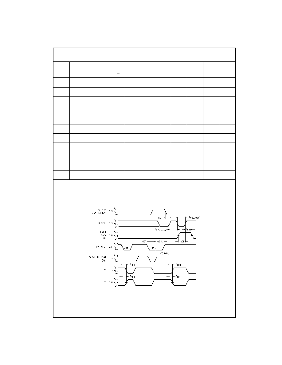
Switching Time Waveform
Note A: The remaining six data and the serial input are LOW.
Note B: Prior to test, HIGH level data is loaded into the P7 input.
Symbol
Parameter
Conditions
Min
Typ
Max
Units
t
pd0
, t
pd1
Propagation Delay Time to a Logical "0" or
V
CC
=
5V
200
400
ns
Logical "1" from Clock or Load to Q or Q
V
CC
=
10V
80
200
ns
t
pd0
, t
pd1
Propagation Delay Time to a Logical "0" or
V
CC
=
5V
200
400
ns
Logical "1" from H to Q or Q
V
CC
=
10V
80
200
ns
t
S
Clock Inhibit Set-up Time
V
CC
=
5V
150
75
ns
V
CC
=
10V
60
30
ns
t
S
Serial Input Set-up Time
V
CC
=
5V
50
25
ns
V
CC
=
10V
30
15
ns
t
H
Serial Input Hold Time
V
CC
=
5V
50
0
ns
V
CC
=
10V
30
0
ns
t
S
Parallel Input Set-Up Time
V
CC
=
5V
150
75
ns
V
CC
=
10V
60
30
ns
t
H
Parallel Input Hold Time
V
CC
=
5V
50
0
ns
V
CC
=
10V
30
0
ns
t
W
Minimum Clock Pulse Width
V
CC
=
5V
70
200
ns
V
CC
=
10V
30
100
ns
t
W
Minimum Load Pulse Width
V
CC
=
5V
85
180
ns
V
CC
=
10V
30
90
ns
f
MAX
Maximum Clock Frequency
V
CC
=
5V
2.5
6
MHz
V
CC
=
10V
5
12
MHz
t
r
, t
f
Maximum Clock Rise and Fall Time
V
CC
=
5V
10
µ
s
V
CC
=
10V
5
µ
s
C
IN
Input Capacitance
(Note 3)
5
pF
C
PD
Power Dissipation Capacitance
(Note 4)
65
pF
5
www.fairchildsemi.com
MM74C165
Logic Waveform