 | –≠–ª–µ–∫—Ç—Ä–æ–Ω–Ω—ã–π –∫–æ–º–ø–æ–Ω–µ–Ω—Ç: MM74C174 | –°–∫–∞—á–∞—Ç—å:  PDF PDF  ZIP ZIP |
October 1987
Revised January 1999
MM74C174 He
x D-T
ype Fli
p
-Fl
o
p
© 1999 Fairchild Semiconductor Corporation
DS005899.prf
www.fairchildsemi.com
MM74C174
Hex D-Type Flip-Flop
General Description
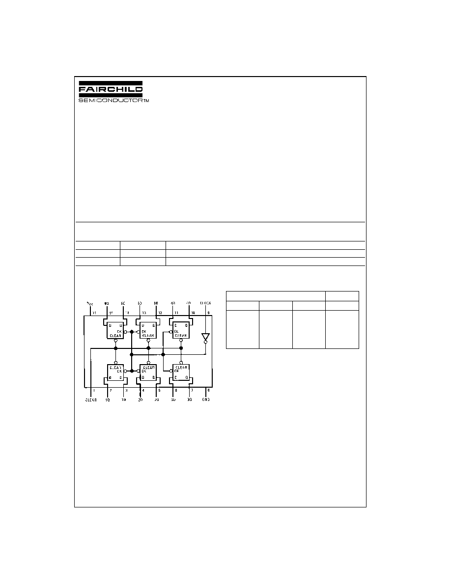
The MM74C174 hex D-type flip-flop is a monolithic comple-
mentary MOS (CMOS) integrated circuit constructed with
N- and P-channel enhancement transistors. All have a
direct clear input. Information at the D inputs meeting the
setup time requirements is transferred to the Q outputs on
the positive-going edge of the clock pulse. Clear is inde-
pendent of clock and accomplished by a low level at the
clear input. All inputs are protected by diodes to V
CC
and
GND.
Features
s
Wide supply voltage range:
3.0V to 15V
s
Guaranteed noise margin:
1.0V
s
High noise immunity:
0.45 V
CC
(typ.)
s
Low power TTL compatibility:
Fan out of 2 driving 74L
Ordering Code:
Device also available in Tape and Reel. Specify by appending suffix letter "X" to the ordering code.
Connection Diagram
Pin Assignments for DIP and SOIC
Top View
Truth Table
Order Number
Package Number
Package Description
MM74C174M
M16A
16-Lead Small Outline Integrated Circuit (SOIC), JEDEC MS-012, 0.150" Narrow
MM74C174N
N16E
16-Lead Plastic Dual-In-Line Package (PDIP), JEDEC MS-001, 0.300" Wide
Inputs
Output
Clear
Clock
D
Q
L
X
X
L
H
H
H
H
L
L
H
L
X
Q
www.fairchildsemi.com
2
M
M
74C174
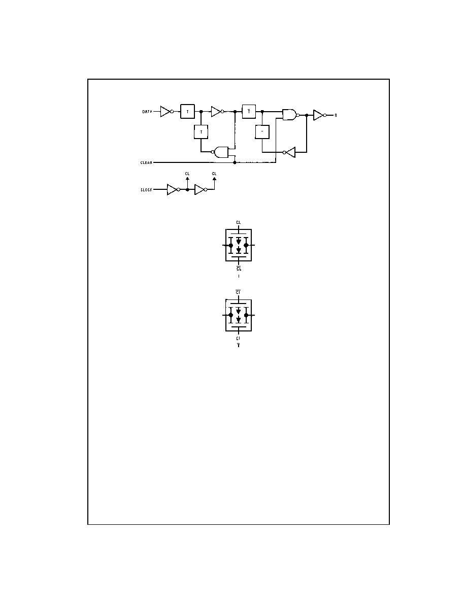
Logic Diagrams
3
www.fairchildsemi.com
MM74C174
Absolute Maximum Ratings
(Note 1)
Note 1: "Absolute Maximum Ratings" are those values beyond which the
safety of the device cannot be guaranteed. Except for "Operating Tempera-
ture Range" they are not meant to imply that the devices should be oper-
ated at these limits. The Electrical Characteristics table provides conditions
for actual device operation.
DC Electrical Characteristics
Min/Max limits apply across temperature range unless otherwise specified
Voltage at Any Pin
-
0.3V to V
CC
+
0.3V
Operating Temperature Range
-
40
∞
C to
+
85
∞
C
Storage Temperature Range
-
65
∞
C to
+
150
∞
C
Power Dissipation (P
D
)
Dual-In-Line
700 mW
Small Outline
500 mW
Operating V
CC
Range
3.0V to 15V
Absolute Maximum V
CC
18V
Lead Temperature
(Soldering, 10 seconds)
260
∞
C
Symbol
Parameter
Conditions
Min
Typ
Max
Units
CMOS TO CMOS
V
IN(1)
Logical "1" Input Voltage
V
CC
=
5V
3.5
V
V
CC
=
10V
8.0
V
V
IN(0)
Logical "0" Input Voltage
V
CC
=
5V
1.5
V
V
CC
=
10V
2.0
V
V
OUT(1)
Logical "1" Output Voltage
V
CC
=
5V, I
O
=
-
10
µ
A
4.5
V
V
CC
=
10V, I
O
=
-
10
µ
A
9.0
V
V
OUT(0)
Logical "0" Output Voltage
V
CC
=
5V, I
O
=
10
µ
A
0.5
V
V
CC
=
10V, I
O
=
10
µ
A
1.0
V
I
IN(1)
Logical "1" Input Current
V
CC
=
15V, V
IN
=
15V
0.005
1.0
µ
A
I
IN(0)
Logical "0" Input Current
V
CC
=
15V, V
IN
=
0V
-
1.0
-
0.005
µ
A
I
CC
Supply Current
V
CC
=
15V
0.05
300
µ
A
CMOS/LPTTL INTERFACE
V
IN(1)
Logical "1" Input Voltage
V
CC
=
4.75V
V
CC
-
1.5
V
V
IN(0)
Logical "0" Input Voltage
V
CC
=
4.75V
0.8
V
V
OUT(1)
Logical "1" Output Voltage
V
CC
=
4.75V, I
O
=
-
360
µ
A
2.4
V
V
OUT(0)
Logical "0" Output Voltage
V
CC
=
4.75V, I
O
=
360
µ
A
0.4
V
OUTPUT DRIVE (See Family Characteristics Data Sheet) (short circuit current)
I
SOURCE
Output Source Current
V
CC
=
5V
-
1.75
-
3.3
mA
(P-Channel)
T
A
=
25
∞
C, V
OUT
=
0V
I
SOURCE
Output Source Current
V
CC
=
10V
-
8.0
-
15
mA
(P-Channel)
T
A
=
25
∞
C, V
OUT
=
0V
I
SINK
Output Sink Current
V
CC
=
5V
1.75
3.6
mA
(N-Channel)
T
A
=
25
∞
C, V
OUT
=
0V
I
SINK
Output Sink Current
V
CC
=
5V
8.0
16
mA
(N-Channel)
T
A
=
25
∞
C, V
OUT
=
0V
www.fairchildsemi.com
4
M
M
74C174
AC Electrical Characteristics
(Note 2)
T
A
=
25
∞
C, C
L
=
50 pF, unless otherwise noted
Note 2: AC Parameters are guaranteed by DC correlated testing.
Note 3: Capacitance is guaranteed by periodic testing.
Note 4: C
PD
determines the no load AC power consumption of any CMOS device. For complete explanation see Family Characteristics Application Note
AN-90.
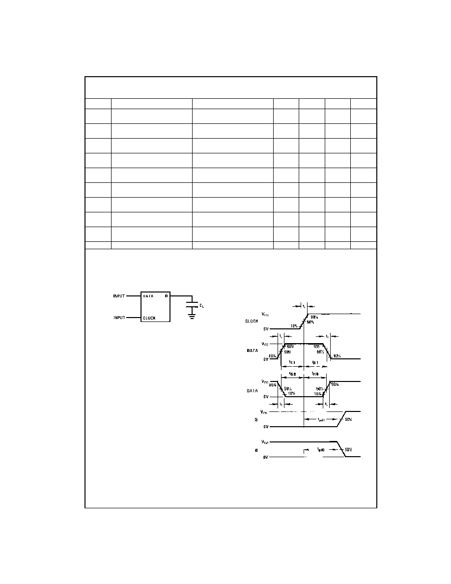
AC Test Circuit
Switching Time Waveforms
CMOS to CMOS
t
r
=
t
f
=
20 ns
Symbol
Parameter
Conditions
Min
Typ
Max
Units
t
pd
Propagation Delay Time to a Logical
V
CC
=
5V
150
300
ns
"0" or Logical "1" from Clock to Q
V
CC
=
10V
70
110
ns
t
pd
Propagation Delay Time to
V
CC
=
5V
110
300
ns
a Logical "0" from Clear
V
CC
=
10V
50
110
ns
t
S1
, t
S0
Time Prior to Clock Pulse that
V
CC
=
5V
75
ns
Data Must be Present
V
CC
=
10V
25
ns
t
H1
, t
H0
Time after Clock Pulse
V
CC
=
5V
0
-
10
ns
that Data Must be Held
V
CC
=
10V
0
-
5.0
ns
t
W
Minimum Clock Pulse Width
V
CC
=
5V
50
250
ns
V
CC
=
10V
35
100
ns
t
W
Minimum Clear Pulse Width
V
CC
=
5V
65
140
ns
V
CC
=
10V
35
70
ns
t
r
, t
f
Maximum Clock Rise and
V
CC
=
5V
15
>
1200
µ
s
Fall Time
V
CC
=
10V
5.0
>
1200
µ
s
f
MAX
Maximum Clock Frequency
V
CC
=
5V
2.0
6.5
MHz
V
CC
=
10V
5.0
12
MHz
C
IN
Input Capacitance
Clear Input (Note 3)
11
pF
Any Other Input
5.0
pF
C
PD
Power Dissipation Capacitance
Per Package (Note 4)
95
pF
5
www.fairchildsemi.com
MM74C174
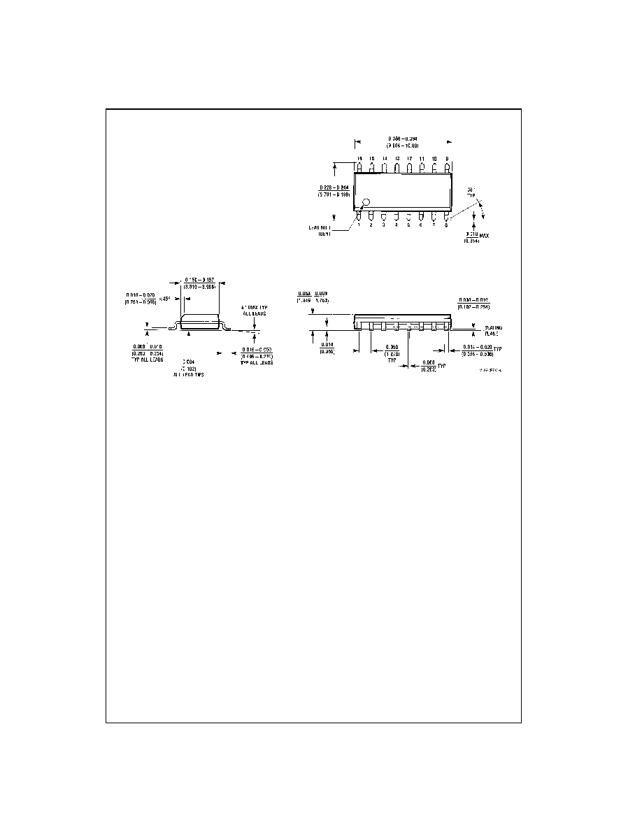
Physical Dimensions
inches (millimeters) unless otherwise noted
16-Lead Small Outline Integrated Circuit (SOIC), JEDEC MS-012, 0.150" Narrow
Package Number M16A