 | –≠–ª–µ–∫—Ç—Ä–æ–Ω–Ω—ã–π –∫–æ–º–ø–æ–Ω–µ–Ω—Ç: MM74C32M | –°–∫–∞—á–∞—Ç—å:  PDF PDF  ZIP ZIP |
October 1987
Revised January 1999
MM74C32
Q
u
ad 2-
Inp
u
t
O
R
Gate
© 1999 Fairchild Semiconductor Corporation
DS005881.prf
www.fairchildsemi.com
MM74C32
Quad 2-Input OR Gate
General Description
The MM74C32 employs complementary MOS (CMOS)
transistors to achieve low power and high noise margin,
these gates provide the basic functions used in the imple-
mentation of digital integrated circuit systems. The N- and
P-channel enhancement mode transistors provide a sym-
metrical circuit with output swings essentially equal to the
supply voltage. This results in high noise immunity over a
wide supply voltage range. No DC power other than that
caused by leakage current is consumed during static con-
ditions. All inputs are protected against static discharge
damage.
Features
s
Wide supply voltage range:
3.0V to 15V
s
Guaranteed noise margin:
1.0V
s
High noise immunity:
0.45V V
CC
(typ.)
s
Low power TTL compatibility:
fan out of 2 driving 74L
Ordering Code:
Devices also available in Tape and Reel. Specify by appending suffix letter "X" to the ordering code.
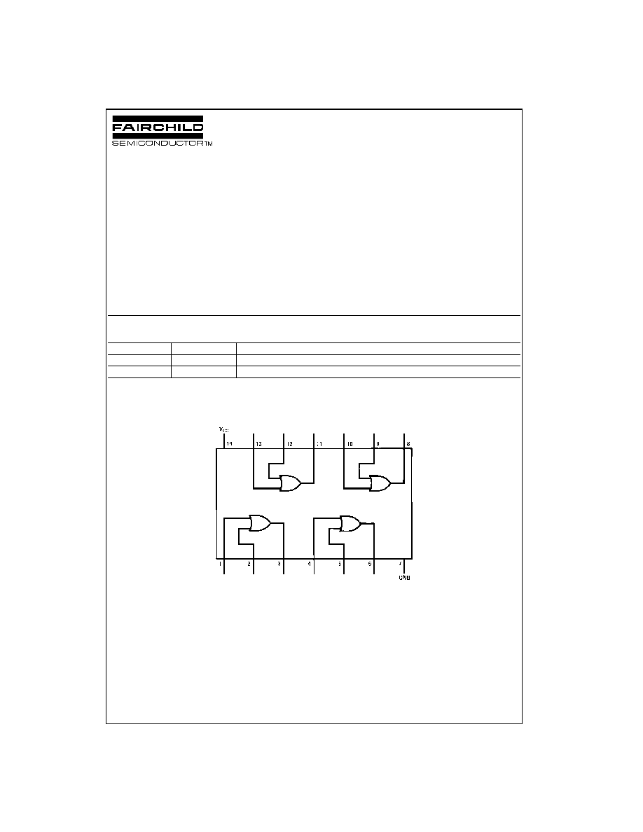
Connection Diagram
Pin Assignments for DIP and SOIC
Top View
Order Number
Package Number
Package Description
MM74C32M
M14A
14-Lead Small Outline Integrated Circuit (SOIC), JEDEC MS-120, 0.150" Narrow
MM74C32N
N14A
14-Lead Plastic Dual-In-Line Package (PDIP), JEDEC MS-001, 0.300" Wide
www.fairchildsemi.com
2
MM
74C32
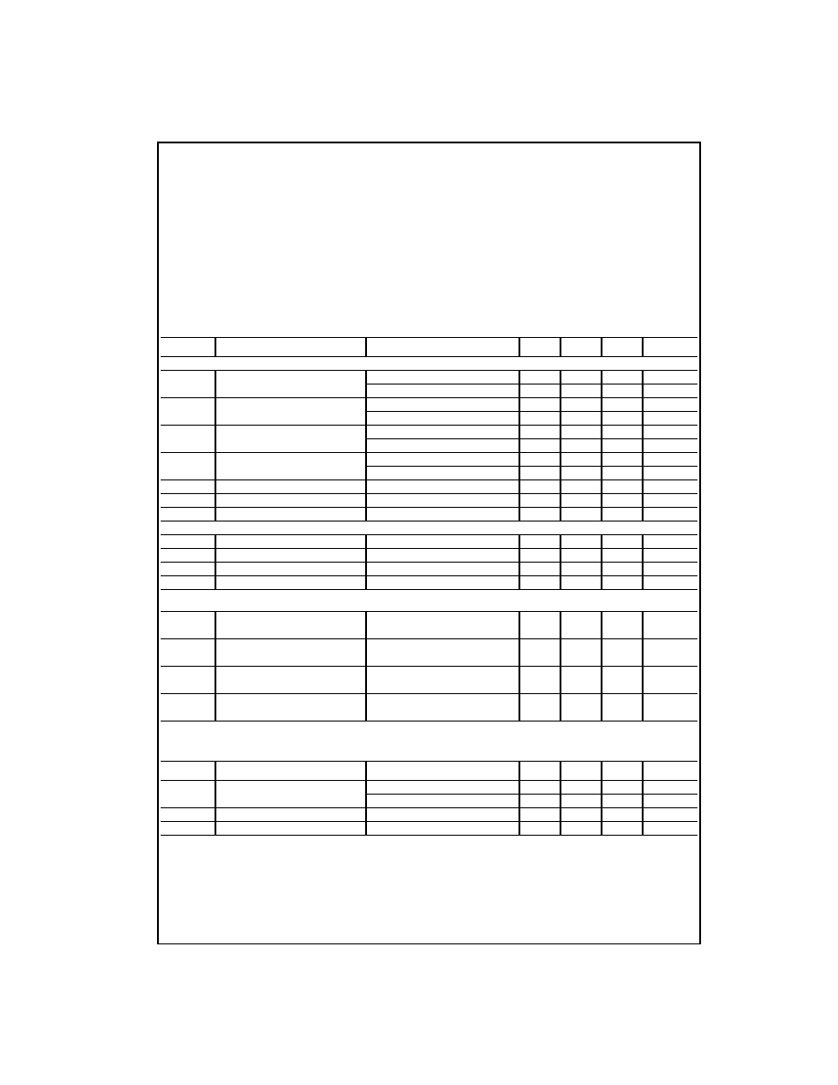
Absolute Maximum Ratings
(Note 1)
Note 1: "Absolute Maximum Ratings" are those values beyond which the
safety of the device cannot be guaranteed. Except for "Operating Tempera-
ture Range" they are not meant to imply that the devices should be oper-
ated at these limits. The Electrical Characteristics table provides conditions
for actual device operation.
DC Electrical Characteristics
Min/Max limits apply across temperature range unless otherwise noted
AC Electrical Characteristics
(Note 2)
T
A
=
25
∞
C, C
L
=
50 pF, unless otherwise specified
Note 2: AC Parameters are guaranteed by DC correlated testing.
Note 3: Capacitance is guaranteed by periodic testing.
Note 4: C
PD
determines the no load AC power consumption of any CMOS device. For complete explanation see Family Characteristics Application Note--
AN-90.
Voltage at Any Pin
-
0.3V to V
CC
+
0.3V
Operating Temperature Range
-
40
∞
C to
+
85
∞
C
Storage Temperature Range
-
65
∞
C to
+
150
∞
C
Power Dissipation (P
D
)
Dual-In-Line
700 mW
Small Outline
500 mW
Operating V
CC
Range
3.0V to 15V
Absolute Maximum V
CC
18V
Lead Temperature
(Soldering, 10 seconds)
260
∞
C
Symbol
Parameter
Conditions
Min
Typ
Max
Units
CMOS TO CMOS
V
IN(1)
Logical "1" Input Voltage
V
CC
=
5.0V
3.5
V
V
CC
=
10V
8.0
V
V
IN(0)
Logical "0" Input Voltage
V
CC
=
5.0V
1.5
V
V
CC
=
10V
2.0
V
V
OUT(1)
Logical "1" Output Voltage
V
CC
=
5.0V, I
O
=
-
10
µ
A
4.5
V
V
CC
=
10V, I
O
=
-
10
µ
A
9.0
V
V
OUT(0)
Logical "0" Output Voltage
V
CC
=
5.0V, I
O
=
10
µ
A
0.5
V
V
CC
=
10V, I
O
=
10
µ
A
1.0
V
I
IN(1)
Logical "1" Input Current
V
CC
=
15V, V
IN
=
15V
0.005
1.0
µ
A
I
IN(0)
Logical "0" Input Current
V
CC
=
15V, V
IN
=
0V
-
1.0
-
0.005
µ
A
I
CC
Supply Current
V
CC
=
15V
0.05
15
µ
A
CMOS/LPTTL INTERFACE
V
IN(1)
Logical "1" Input Voltage
V
CC
=
4.75V
V
CC
-
1.5
V
V
IN(0)
Logical "0" Input Voltage
V
CC
=
4.75V
0.8
V
V
OUT(1)
Logical "1" Output Voltage
V
CC
=
4.75V, I
O
=
-
360
µ
A
2.4
V
V
OUT(0)
Logical "0" Output Voltage
V
CC
=
4.75V, I
O
=
360
µ
A
0.4
V
OUTPUT DRIVE (see Family Characteristics Data Sheet) T
A
=
25
∞
C (short circuit current)
I
SOURCE
Output Source Current
V
CC
=
5.0V, V
OUT
=
0V
-
1.75
-
3.3
mA
(P-Channel)
I
SOURCE
Output Source Current
V
CC
=
10V, V
OUT
=
0V
-
8.0
-
15
mA
(P-Channel)
I
SINK
Output Sink Current
V
CC
=
5.0V, V
OUT
=
V
CC
1.75
3.6
mA
(N-Channel)
I
SINK
Output Sink Current
V
CC
=
10V, V
OUT
=
V
CC
8.0
16
mA
(N-Channel)
Symbol
Parameter
Conditions
Min
Typ
Max
Units
t
pd
Propagation Delay Time to
V
CC
=
5.0V
80
150
ns
Logical "1" or "0"
V
CC
=
10V
35
70
ns
C
IN
Input Capacitance
Any Input (Note 3)
5
pF
C
PD
Power Dissipation Capacitance
Per Gate (Note 4)
15
pF
3
www.fairchildsemi.com
MM74C32
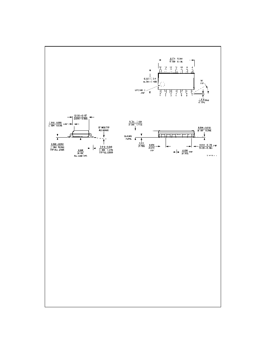
Physical Dimensions
inches (millimeters) unless otherwise noted
14-Lead Small Outline Integrated Circuit (SOIC), JEDEC MS-120, 0.150" Narrow
Package Number M14A
Fairchild does not assume any responsibility for use of any circuitry described, no circuit patent licenses are implied and Fairchild reserves the right at any time without notice to change said circuitry and specifications.
M
M
74C32 Quad
2
-
I
nput OR
Gate
LIFE SUPPORT POLICY
FAIRCHILD'S PRODUCTS ARE NOT AUTHORIZED FOR USE AS CRITICAL COMPONENTS IN LIFE SUPPORT
DEVICES OR SYSTEMS WITHOUT THE EXPRESS WRITTEN APPROVAL OF THE PRESIDENT OF FAIRCHILD
SEMICONDUCTOR CORPORATION. As used herein:
1. Life support devices or systems are devices or systems
which, (a) are intended for surgical implant into the
body, or (b) support or sustain life, and (c) whose failure
to perform when properly used in accordance with
instructions for use provided in the labeling, can be rea-
sonably expected to result in a significant injury to the
user.
2. A critical component in any component of a life support
device or system whose failure to perform can be rea-
sonably expected to cause the failure of the life support
device or system, or to affect its safety or effectiveness.
www.fairchildsemi.com
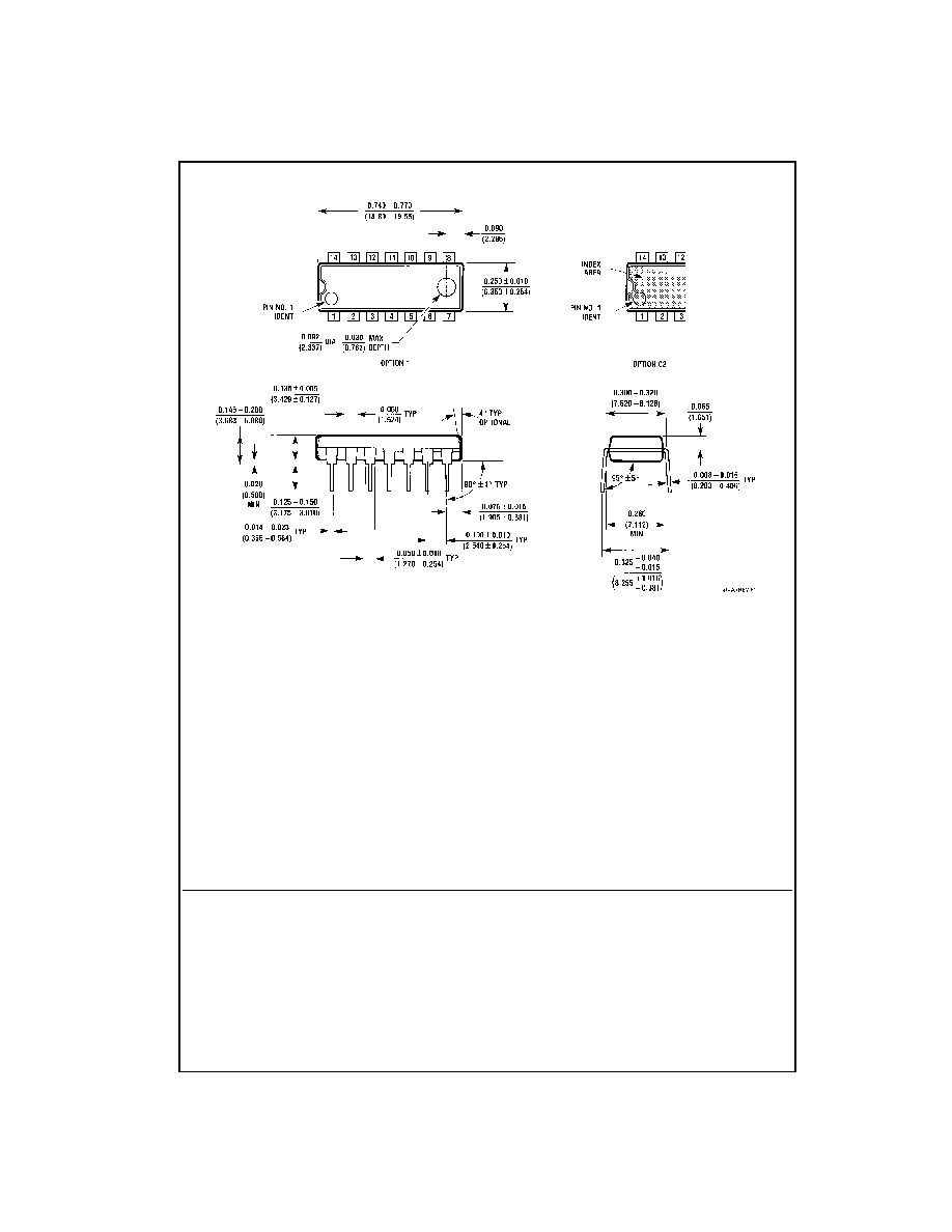
Physical Dimensions
inches (millimeters) unless otherwise noted (Continued)
14-Lead Plastic Dual-In-Line Package (PDIP), JEDEC MS-001, 0.300" Wide
Package Number N14A