© 2002 Fairchild Semiconductor Corporation
DS005906
www.fairchildsemi.com
October 1987
Revised May 2002
MM74C373 ∑
MM74C374 3-ST
A
T
E
Oct
a
l D-T
y
pe Lat
c
h
∑ 3-ST
A
T
E
Oct
a
l D-T
y
pe Fl
ip-
F
lop
MM74C373 ∑ MM74C374
3-STATE Octal D-Type Latch ∑
3-STATE Octal D-Type Flip-Flop
General Description
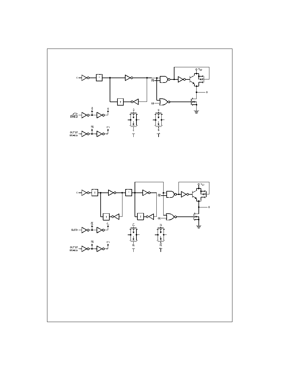
The MM74C373 and MM74C374 are integrated, comple-
mentary MOS (CMOS), 8-bit storage elements with 3-
STATE outputs. These outputs have been specially
designed to drive high capacitive loads, such as one might
find when driving a bus, and to have a fan out of 1 when
driving standard TTL. When a high logic level is applied to
the OUTPUT DISABLE input, all outputs go to a high
impedance state, regardless of what signals are present at
the other inputs and the state of the storage elements.
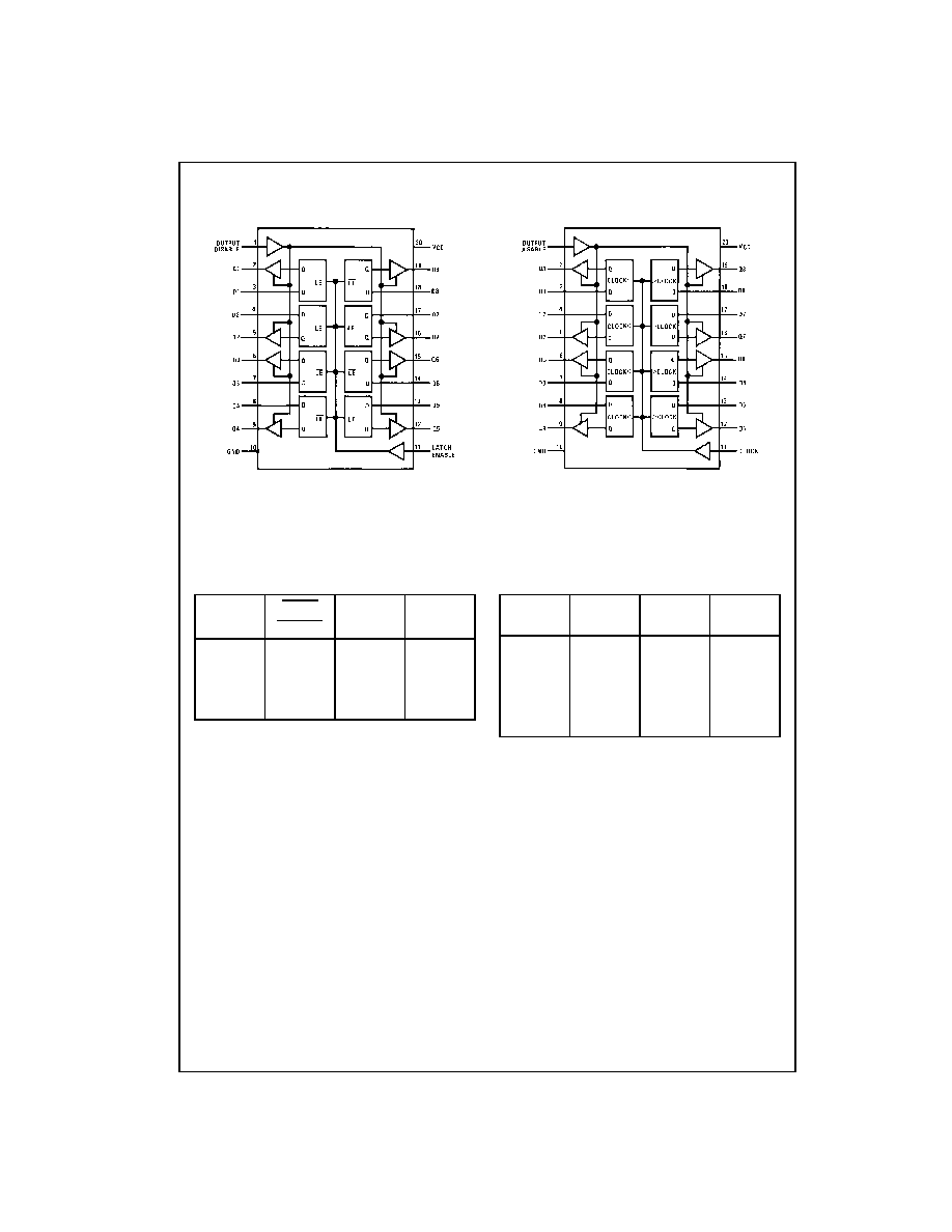
The MM74C373 is an 8-bit latch. When LATCH ENABLE is
high, the Q outputs will follow the D inputs. When LATCH
ENABLE goes low, data at the D inputs, which meets the
set-up and hold time requirements, will be retained at the
outputs until LATCH ENABLE returns high again.
The MM74C374 is an 8-bit, D-type, positive-edge triggered
flip-flop. Data at the D inputs, meeting the set-up and hold
time requirements, is transferred to the Q outputs on posi-
tive-going transitions of the CLOCK input.
Both the MM74C373 and the MM74C374 are being assem-
bled in 20-pin dual-in-line packages with 0.300" pin cen-
ters.
Features
s
Wide supply voltage range:
3V to 15V
s
High noise immunity:
0.45 V
CC
(typ.)
s
Low power consumption
s
TTL compatibility:
Fan out of 1driving standard TTL
s
Bus driving capability
s
3-STATE outputs
s
Eight storage elements in one package
s
Single CLOCK/LATCH ENABLE and OUTPUT DIS-
ABLE control inputs
s
20-pin dual-in-line package with 0.300" centers takes
half the board space of a 24-pin package
Ordering Code:
Devices also available in Tape and Reel. Specify by appending the suffix letter "X" to the ordering code.
Order Number
Package Number
Package Description
MM74C373M
M20B
20-Lead Small Outline Integrated Circuit (SOIC), JEDEC MS-013, 0.300" Wide
MM74C373N
N20A
20-Lead Plastic Dual-In-Line Package (PDIP), JEDEC MS-001, 0.300" Wide
MM74C374M
M20B
20-Lead Small Outline Integrated Circuit (SOIC), JEDEC MS-013, 0.300" Wide
MM74C374N
N20A
20-Lead Plastic Dual-In-Line Package (PDIP), JEDEC MS-001, 0.300" Wide
www.fairchildsemi.com
4
MM
74
C
3
7
3
∑
M
M
74C374
Absolute Maximum Ratings
(Note 1)
Note 1: "Absolute Maximum Ratings" are those values beyond which the
safety of the device cannot be guaranteed. Except for "Operating Tempera-
ture Range" they are not meant to imply that the devices should be oper-
ated at these limits. The table of "Electrical Characteristics" provides
conditions for actual device operation.
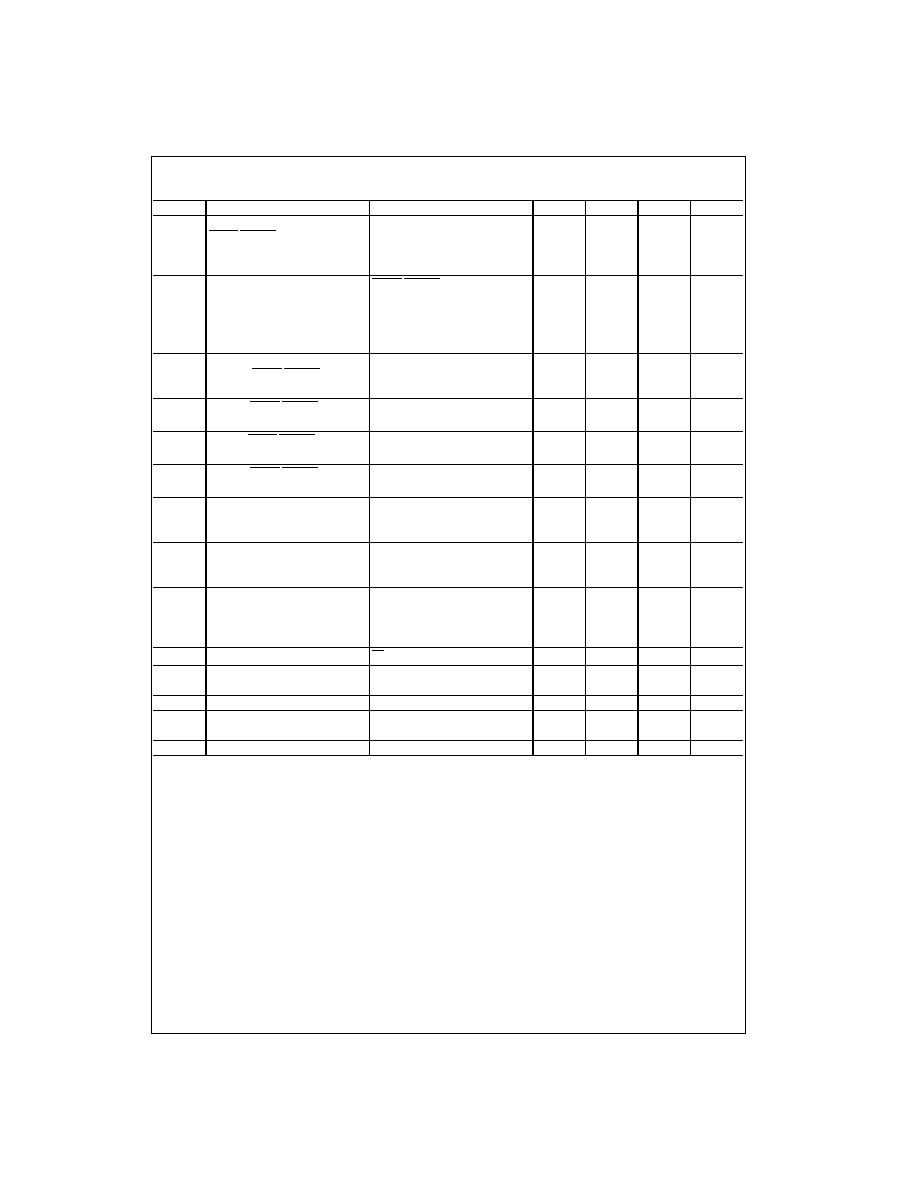
DC Electrical Characteristics
Min/Max limits apply across temperature range unless otherwise noted
Note 2: These are peak output current capabilities. Continuous output current is rated at 12 mA max.
Voltage at Any Pin
-
0.3V to V
CC
+
0.3V
Operating Temperature Range (T
A
)
MM74C373
-
55
∞
C to
+
125
∞
C
Storage Temperature Range (T
S
)
-
65
∞
C to
+
150
∞
C
Power Dissipation
Dual-In-Line
700 mW
Small Outline
500 mW
Operating V
CC
Range
3V to 15V
Absolute Maximum V
CC
18V
Lead Temperature (T
L
)
(Soldering, 10 seconds)
260
∞
C
Symbol
Parameter
Conditions
Min
Typ
Max
Units
CMOS TO CMOS
V
IN(1)
Logical "1" Input Voltage
V
CC
=
5V
3.5
V
V
CC
=
10V
8.0
V
IN(0)
Logical "0" Input Voltage
V
CC
=
5V
1.5
V
V
CC
=
10V
2.0
V
OUT(1)
Logical "1" Output Voltage
V
CC
=
5V, I
O
=
-
10
µ
A
4.5
V
V
CC
=
10V, I
O
=
-
10
µ
A
9.0
V
OUT(0)
Logical "0" Output Voltage
V
CC
=
5V, I
O
=
10
µ
A
0.5
V
V
CC
=
10V, I
O
=
10
µ
A
1.0
I
IN(1)
Logical "1" Input Current
V
CC
=
15V, V
IN
=
15V
0.005
1.0
µ
A
I
IN(0)
Logical "0" Input Current
V
CC
=
15V, V
IN
=
0V
-
1.0
-
0.005
µ
A
I
OZ
3-STATE Leakage Current
V
CC
=
15V, V
O
=
15V
0.005
1.0
µ
A
V
CC
=
15V, V
O
=
0V
-
1.0
-
0.005
I
CC
Supply Current
V
CC
=
15V
0.05
300
µ
A
CMOS/LPTTL INTERFACE
V
IN(1)
Logical "1" Input Voltage
V
CC
=
4.75V
V
CC
-
1.5
V
V
IN(0)
Logical "0" Input Voltage
V
CC
=
4.75V
0.8
V
V
OUT(1)
Logical "1" Output Voltage
V
CC
=
4.75V, I
O
=
-
360
µ
A
V
CC
-
0.4
V
V
CC
=
4.75V, I
O
=
-
1.6 mA
2.4
V
V
OUT(0)
Logical "0" Output Voltage
V
CC
=
4.75V, I
O
=
1.6 mA
0.4
V
OUTPUT DRIVE (Short Circuit Current)
I
SOURCE
Output Source Current
V
CC
=
5V, V
OUT
=
0V
-
12
-
24
mA
T
A
=
25
∞
C (Note 2)
I
SOURCE
Output Source Current
V
CC
=
10V, V
OUT
=
0V
-
24
-
48
mA
T
A
=
25
∞
C (Note 2)
I
SINK
Output Sink Current
V
CC
=
5V, V
OUT
=
V
CC
6
12
mA
(N-Channel)
T
A
=
25
∞
C (Note 2)
I
SINK
Output Sink Current
V
CC
=
10V, V
OUT
=
V
CC
24
48
mA
(N-Channel)
T
A
=
25
∞
C (Note 2)
5
www.fairchildsemi.com
MM74C373
∑
MM74C374
AC Electrical Characteristics
(Note 3)
MM74C373, T
A
=
25
∞
C, C
L
=
50 pF, t
r
=
t
f
=
20 ns, unless otherwise noted
Note 3: AC Parameters are guaranteed by DC correlated testing.
Note 4: Capacitance is guaranteed by periodic testing.
Note 5: C
PD
determines the no load AC power consumption of any CMOS device. For complete explanation see Family Characteristics Application Note
AN-90.
Symbol
Parameter
Conditions
Min
Typ
Max
Units
t
pd0
, t
pd1
Propagation Delay,
V
CC
=
5V, C
L
=
50 pF
165
330
ns
LATCH ENABLE to Output
V
CC
=
10V, C
L
=
50 pF
70
140
V
CC
=
5V, C
L
=
150 pF
195
390
V
CC
=
10V, C
L
=
150 pF
85
170
t
pd0
, t
pd1
Propagation Delay Data
LATCH ENABLE
=
V
CC
In to Output
V
CC
=
5V, C
L
=
50 pF
155
310
ns
V
CC
=
10V, C
L
=
50 pF
70
140
V
CC
=
5V, C
L
=
150 pF
185
370
V
CC
=
10V, C
L
=
150 pF
85
170
t
SET-UP
Minimum Set-Up Time Data In
t
HOLD
=
0 ns
to CLOCK/LATCH ENABLE
V
CC
=
5V
70
140
ns
V
CC
=
10V
35
70
f
MAX
Maximum LATCH ENABLE
V
CC
=
5V
3.5
6.7
MHz
Frequency
V
CC
=
10V
4.5
9.0
t
PWH
Minimum LATCH ENABLE
V
CC
5V
75
150
ns
Pulse Width
V
CC
=
10V
55
110
t
r
, t
f
Maximum LATCH ENABLE
V
CC
=
5V
NA
µ
s
Rise and Fall Time
V
CC
=
10V
NA
t
1H
, t
0H
Propagation Delay OUTPUT
R
L
=
10k, C
L
=
5 pF
DISABLE to High Impedance
V
CC
=
5V
105
210
ns
State (from a Logic Level)
V
CC
=
10V
60
120
t
H1
, t
H0
Propagation Delay OUTPUT
R
L
=
10k, C
L
=
50 pF
DISABLE to Logic Level
V
CC
=
5V
105
210
ns
(from High Impedance State)
V
CC
=
10V
45
90
t
THL
, t
TLH
Transition Time
V
CC
=
5V, C
L
=
50 pF
65
130
ns
V
CC
=
10V, C
L
=
50 pF
35
70
V
CC
=
5V, C
L
=
150 pF
110
220
V
CC
=
10V, C
L
=
150 pF
70
140
C
LE
Input Capacitance
LE Input (Note 4)
7.5
10
pF
C
OD
Input Capacitance
OUTPUT DISABLE
7.5
10
pF
Input (Note 4)
C
IN
Input Capacitance
Any Other Input (Note 4)
5
7.5
pF
C
OUT
Output Capacitance
High Impedance
10
15
pF
State (Note 4)
C
PD
Power Dissipation Capacitance
Per Package (Note 5)
200
pF