 | –≠–ª–µ–∫—Ç—Ä–æ–Ω–Ω—ã–π –∫–æ–º–ø–æ–Ω–µ–Ω—Ç: MM74C76 | –°–∫–∞—á–∞—Ç—å:  PDF PDF  ZIP ZIP |
© 2002 Fairchild Semiconductor Corporation
DS005884
www.fairchildsemi.com
October 1987
Revised May 2002
MM74C73 ∑
MM74C76 D
u
a
l
J-K Fli
p
-Fl
ops wit
h
Cl
ear and P
r
eset
MM74C73 ∑ MM74C76
Dual J-K Flip-Flops with Clear and Preset
General Description
The MM74C73 and MM74C76 dual J-K flip-flops are mono-
lithic complementary MOS (CMOS) integrated circuits con-
structed with N- and P-channel enhancement transistors.
Each flip-flop has independent J, K, clock and clear inputs
and Q and Q outputs. The MM74C76 flip flops also include
preset inputs and are supplied in 16 pin packages. This
flip-flop is edge sensitive to the clock input and change
state on the negative going transition of the clock pulse.
Clear or preset is independent of the clock and is accom-
plished by a low level on the respective input.
Features
s
Supply voltage range:
3V to 15V
s
Tenth power TTL compatible:
Drive 2 LPTTL loads
s
High noise immunity:
0.45 V
CC
(typ.)
s
Low power:
50 nW (typ.)
s
Medium speed operation:
10 MHz (typ.)
Applications
∑ Automotive
∑ Data terminals
∑ Instrumentation
∑ Medical electronics
∑ Alarm systems
∑ Industrial electronics
∑ Remote metering
∑ Computers
Ordering Code:
Devices also available in Tape and Reel. Specify by appending suffix letter "X" to the ordering code.
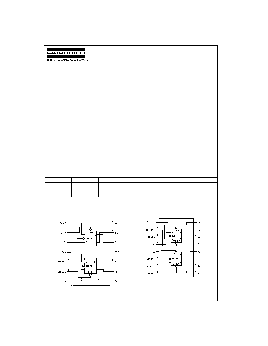
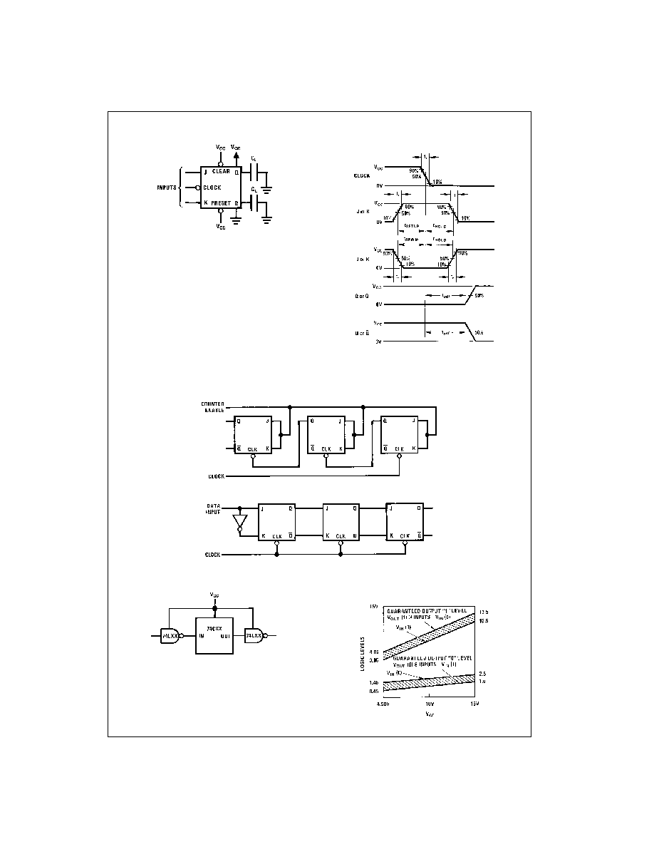
Connection Diagrams
MM74C73
Note: A logic "0" on clear sets Q to logic "0".
Top View
MM74C76
Note: A logic "0" on clear sets Q to a logic "0".
Note: A logic "0" on preset sets Q to a logic "1".
Top View
Order Number
Package Number
Package Description
MM74C73N
N14A
14-Lead Plastic Dual-In-Line Package (PDIP), JEDEC MS-001, 0.300" Wide
MM74C76M
M16A
16-Lead Small Outline Integrated Circuit (SOIC), JEDEC MS-012, 0.150" Narrow
MM74C76N
N16E
16-Lead Plastic Dual-In-Line Package (PDIP), JEDEC MS-001, 0.300" Wide
www.fairchildsemi.com
2
MM74C73
∑
MM
74C76
Truth Table
t
n
=
bit time before clock pulse
t
n
+
1
=
bit time after clock pulse
Note 1: No change in output from previous state
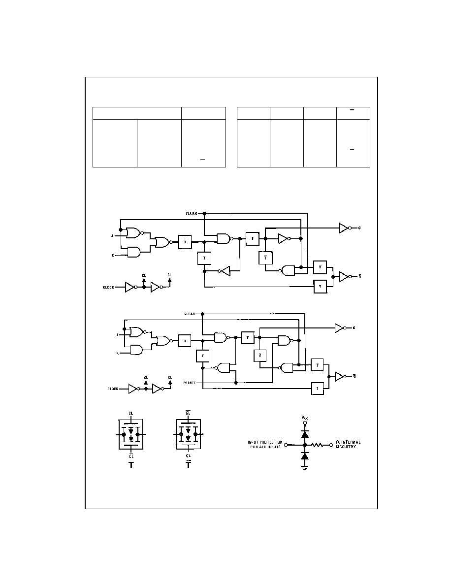
Logic Diagrams
MM74C73
MM74C76
Transmission Gate
t
n
t
n
+
1
Preset
Clear
Q
n
Q
n
J
K
Q
0
0
0
0
0
0
Q
n
0
1
1
0
0
1
0
1
0
0
1
1
0
1
1
1
Q
n
Q
n
1
1
Q
n
(Note 1)
(Note 1)
3
www.fairchildsemi.com
MM74C73
∑
MM74C76
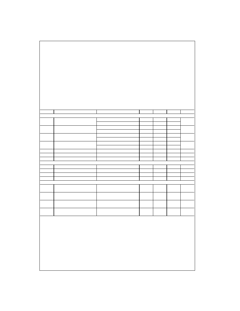
Absolute Maximum Ratings
(Note 2)
Note 2: "Absolute Maximum Ratings" are those values beyond which the
safety of the device cannot be guaranteed. Except for "Operating Tempera-
ture Range" they are not meant to imply that the devices should be oper-
ated at these limits. The table of Electrical Characteristics provides
conditions for actual device operation.
DC Electrical Characteristics
Min/Max limits apply across temperature range unless otherwise noted
Voltage at Any Pin
-
0.3V to V
CC
+
0.3V
Operating Temperature Range
-
55
∞
C to
+
125
∞
C
Storage Temperature
-
65
∞
C to
+
150
∞
C
Power Dissipation
Dual-In-Line
700 mW
Small Outline
500 mW
Lead Temperature
(Soldering, 10 seconds)
260
∞
C
Operating V
CC
Range
+
3V to 15V
V
CC
(Max)
18V
Symbol
Parameter
Conditions
Min
Typ
Max
Units
CMOS TO CMOS
V
IN(1)
Logical "1" Input Voltage
V
CC
=
5V
3.5
V
V
CC
=
10V
8
V
IN(0)
Logical "0" Input Voltage
V
CC
=
5V
1.5
V
V
CC
=
10V
2
V
OUT(1)
Logical "1" Output Voltage
V
CC
=
5V
4.5
V
V
CC
=
10V
9
V
OUT(0)
Logical "0" Output Voltage
V
CC
=
5V
0.5
V
V
CC
=
10V
1
I
IN(1)
Logical "1" Input Current
V
CC
=
15V
1
µ
A
I
IN(0)
Logical "0" Input Current
V
CC
=
15V
-
1
µ
A
I
CC
Supply Current
V
CC
=
15V
0.050
60
µ
A
LOW POWER TTL TO CMOS INTERFACE
V
IN(1)
Logical "1" Input Voltage
V
CC
=
4.75V
V
CC
-
1.5
V
V
IN(0)
Logical "0" Input Voltage
V
CC
=
4.75V
0.8
V
V
OUT(1)
Logical "1" Output Voltage
V
CC
=
4.75V, I
O
=
-
360
µ
A
2.4
V
V
OUT(0)
Logical "0" Output Voltage
V
CC
=
4.75V, I
O
=
360
µ
A
0.4
V
OUTPUT DRIVE (See Family Characteristics Data Sheet) (Short Circuit Current)
I
SOURCE
Output Source Current
V
CC
=
5V, V
IN(0)
=
0V
-
1.75
mA
T
A
=
25
∞
C, V
OUT
=
0V
I
SOURCE
Output Source Current
V
CC
=
10V, V
IN(0)
=
0V
-
8
mA
T
A
=
25
∞
C, V
OUT
=
0V
I
SINK
Output Sink Current
V
CC
=
5V, V
IN(1)
=
5V
1.75
mA
T
A
=
25
∞
C, V
OUT
=
V
CC
I
SINK
Output Sink Current
V
CC
=
10V, V
IN(1)
=
10V
8
mA
T
A
=
25
∞
C, V
OUT
=
V
CC
www.fairchildsemi.com
4
MM74C73
∑
MM
74C76
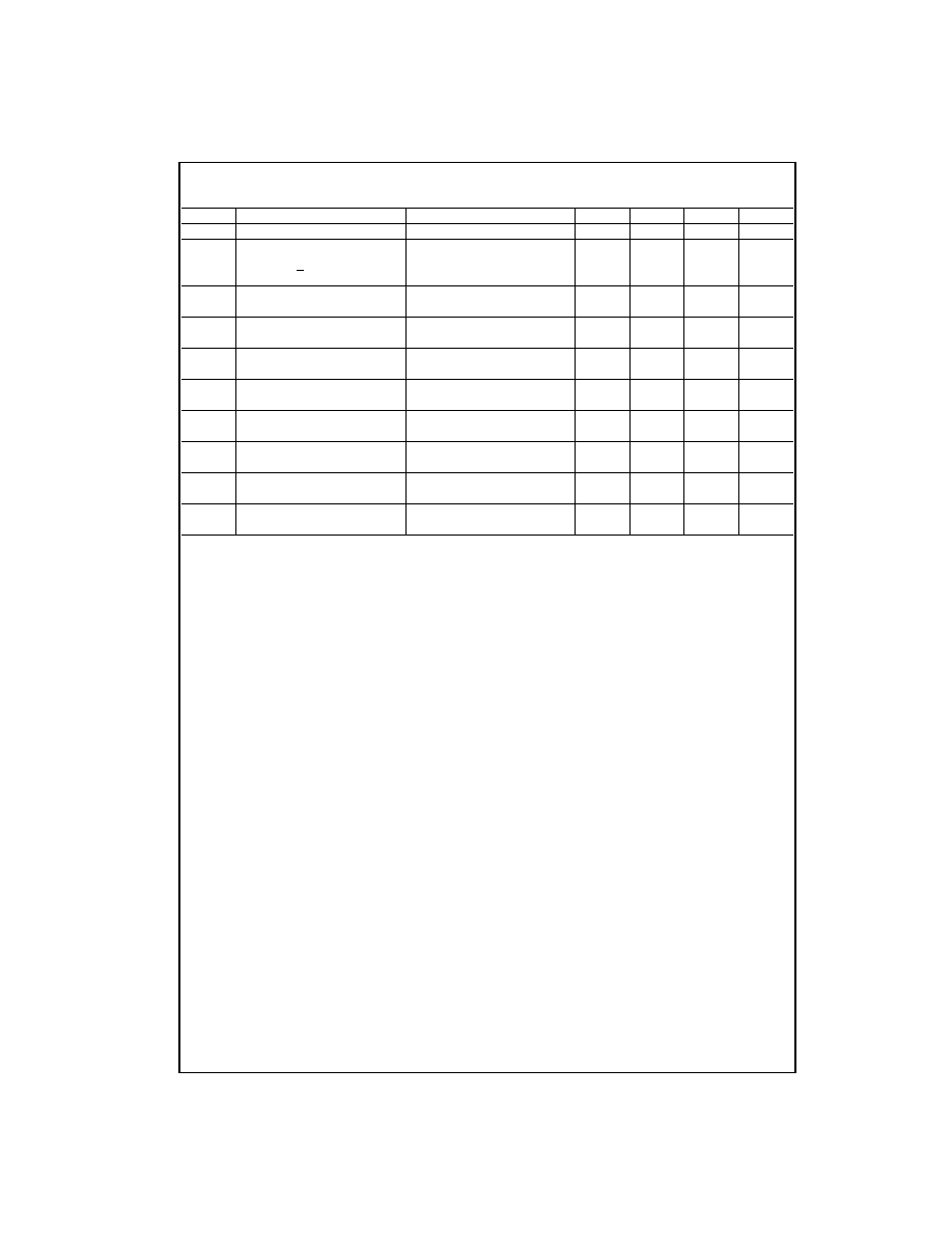
AC Electrical Characteristics
(Note 3)
T
A
=
25
∞
C, C
L
=
50 pF, unless otherwise noted
Note 3: AC Parameters are guaranteed by DC correlated testing.
Symbol
Parameter
Conditions
Min
Typ
Max
Units
C
IN
Input Capacitance
Any Input
5
pF
t
pd0
, t
pd1
Propagation Delay Time to a
V
CC
=
5V
180
300
ns
Logical "0" or Logical "1" from
V
CC
=
10V
70
110
Clock to Q or Q
t
pd0
Propagation Delay Time to a
V
CC
=
5V
200
300
ns
Logical "0" from Preset or Clear
V
CC
=
10V
80
130
t
pd
Propagation Delay Time to a
V
CC
=
5V
200
300
ns
Logical "1" from Preset or Clear
V
CC
=
10V
80
130
t
S
Time Prior to Clock Pulse that
V
CC
=
5V
110
175
ns
Data must be Present
V
CC
=
10V
45
70
t
H
Time after Clock Pulse that J
V
CC
=
5V
-
40
0
ns
and K must be Held
V
CC
=
10V
-
20
0
t
PW
Minimum Clock Pulse Width
V
CC
=
5V
120
190
ns
t
WL
=
t
WH
V
CC
=
10V
50
80
t
PW
Minimum Preset and Clear
V
CC
=
5V
90
130
ns
Pulse Width
V
CC
=
10V
40
60
t
MAX
Maximum Toggle Frequency
V
CC
=
5V
2.5
4
MHz
V
CC
=
10V
7
11
t
r
, t
f
Clock Pulse Rise and Fall Time
V
CC
=
5V
15
µ
s
V
CC
=
10V
5
5
www.fairchildsemi.com
MM74C73
∑
MM74C76
AC Test Circuit
Switching Time Waveforms
CMOS to CMOS
t
r
=
t
f
=
20 ns
Typical Applications
Ripple Binary Counters
Shift Registers
74C Compatibility
Guaranteed Noise Margin
as a Function of V
CC