 | –≠–ª–µ–∫—Ç—Ä–æ–Ω–Ω—ã–π –∫–æ–º–ø–æ–Ω–µ–Ω—Ç: MM74C85 | –°–∫–∞—á–∞—Ç—å:  PDF PDF  ZIP ZIP |
© 2002 Fairchild Semiconductor Corporation
DS005886
www.fairchildsemi.com
October 1987
Revised May 2002
MM74C85 4-Bi
t Magnit
ude C
o
m
p
ar
ator
MM74C85
4-Bit Magnitude Comparator
General Description
The MM74C85 is a four-bit magnitude comparator which
will perform comparison of straight binary or BCD codes.
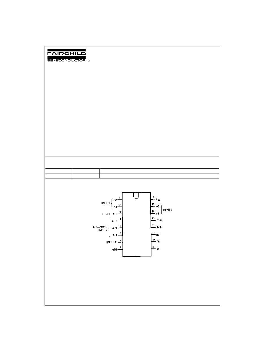
The circuit consists of eight comparing inputs (A0, A1, A2,
A3, B0, B1, B2, B3), three cascading inputs (A
>
B, A
<
B
and A
=
B), and three outputs (A
>
B, A
<
B and A
=
B).
This device compares two four-bit words (A and B) and
determines whether they are "greater than," "less than," or
"equal to" each other by a high level on the appropriate out-
put. For words greater than four-bits, units can be cas-
caded by connecting the outputs (A
>
B, A
<
B, and A
=
B)
of the least significant stage to the cascade inputs (A
>
B, A
<
B and A
=
B) of the next-significant stage. In addition the
least significant stage must have a high level voltage
(V
IN(1)
) applied to the A
=
B input and low level voltage
(V
IN(0)
) applied to A
>
B and A
<
B inputs.
Features
s
Wide supply voltage range:
3.0V to 15V
s
Guaranteed noise margin:
1.0V
s
High noise immunity:
0.4 V
CC
(typ.)
s
Low power:
TTL compatibility:
fan out of 2 driving 74L
s
Expandable to 'N' stages
s
Applicable to binary or BCD
s
Low power pinout: 74L85
Ordering Code:
Connection Diagram
Top View
Order Number
Package Number
Package Description
MM74C85N
N16E
16-Lead Plastic Dual-In-Line Package (PDIP), JEDEC MS-001, 0.300" Wide
www.fairchildsemi.com
2
MM
74C85
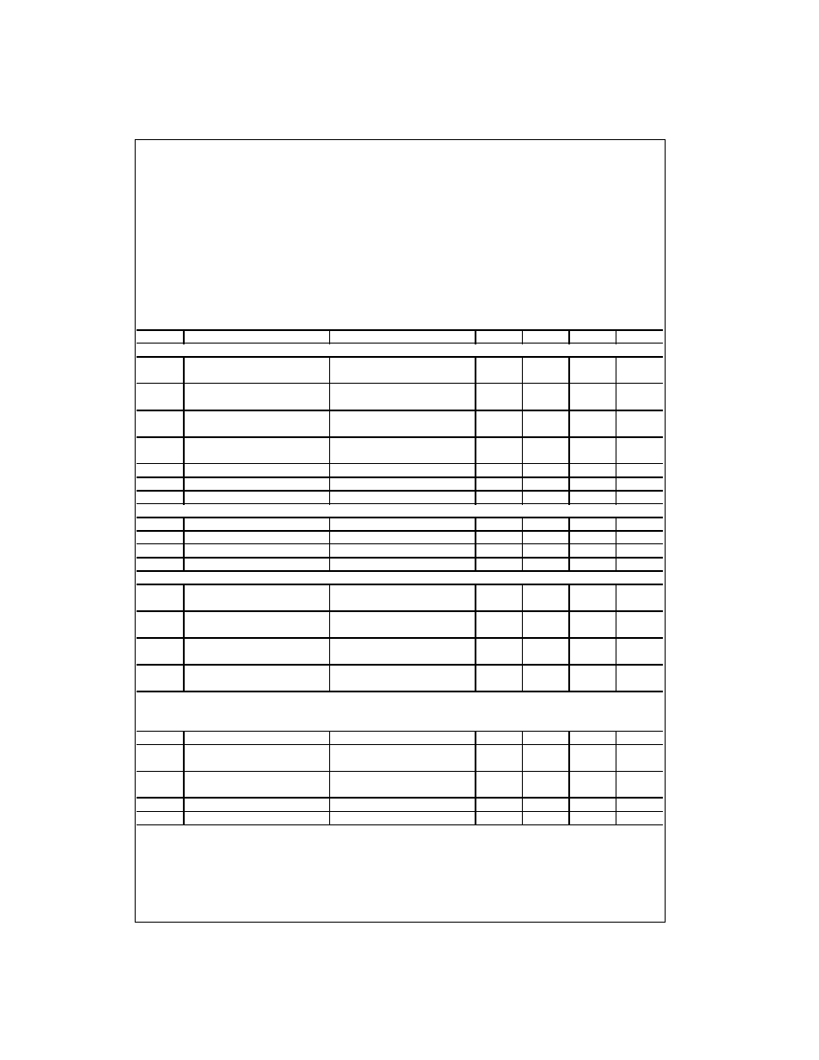
Truth Table
H
=
HIGH Level, L
=
LOW Level, X
=
Irrelevant
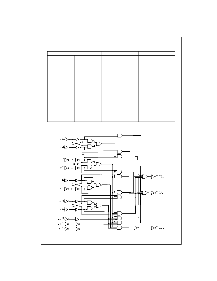
Logic Diagram
Comparing Inputs
Cascading Inputs
Outputs
A3, B3
A2, B2
A1, B1
A0, B0
A
>
B
A
<
B
A
=
B
A
>
B
A
<
B
A
=
B
A3
>
B3
X
X
X
X
X
X
H
L
L
A3
<
B3
X
X
X
X
X
X
L
H
L
A3
=
B3
A2
>
B2
X
X
X
X
X
H
L
L
A3
=
B3
A2
<
B2
X
X
X
X
X
L
H
L
A3
=
B3
A2
=
B2
A1
>
B1
X
X
X
X
H
L
L
A3
=
B3
A2
=
B2
A1
<
B1
X
X
X
X
L
H
L
A3
=
B3
A2
=
B2
A1
=
B1
A0
>
B0
X
X
X
H
L
L
A3
=
B3
A2
=
B2
A1
=
B1
A0
<
B0
X
X
X
L
H
L
A3
=
B3
A2
=
B2
A1
=
B1
A0
=
B0
H
L
L
H
L
L
A3
=
B3
A2
=
B2
A1
=
B1
A0
=
B0
L
H
L
L
H
L
A3
=
B3
A2
=
B2
A1
=
B1
A0
=
B0
L
L
H
L
L
H
A3
=
B3
A2
=
B2
A1
=
B1
A0
=
B0
L
H
H
L
H
H
A3
=
B3
A2
=
B2
A1
=
B1
A0
=
B0
H
L
H
H
L
H
A3
=
B3
A2
=
B2
A1
=
B1
A0
=
B0
H
H
H
H
H
H
A3
=
B3
A2
=
B2
A1
=
B1
A0
=
B0
H
H
L
H
H
L
A3
=
B3
A2
=
B2
A1
=
B1
A0
=
B0
L
L
L
L
L
L
3
www.fairchildsemi.com
MM74C85
Absolute Maximum Ratings
(Note 1)
Note 1: "Absolute Maximum Ratings" are those values beyond which the
safety of the device cannot be guaranteed. Except for "Operating Tempera-
ture Range" they are not meant to imply that the devices should be oper-
ated at these limits. The table of "Electrical Characteristics" provides
conditions for actual device operation.
DC Electrical Characteristics
Min/Max limits apply across temperature range unless otherwise noted
AC Electrical Characteristics
(Note 2)
T
A
=
25
∞
C, C
L
=
50 pF, unless otherwise specified
Note 2: AC Parameters are guaranteed by DC correlated testing.
Note 3: Capacitance is guaranteed by periodic testing.
Note 4: C
PD
determines the no load AC power consumption of any CMOS device. For complete explanation see Family Characteristics application note,
AN-90.
Voltage at Any Pin
-
0.3V to V
CC
+
0.3V
Operating Temperature Range
-
55
∞
C to
+
125
∞
C
Storage Temperature Range
-
65
∞
C to
+
150
∞
C
Power Dissipation (P
D
)
Dual-In-Line
700 mW
Small Outline
500 mW
Operating V
CC
Range
3.0V to 15V
V
CC
18V
Lead Temperature
(Soldering, 10 seconds)
260
∞
C
Symbol
Parameter
Conditions
Min
Typ
Max
Units
CMOS TO CMOS
V
IN(1)
Logical "1" Input Voltage
V
CC
=
5.0V
3.5
V
V
CC
=
10V
8.0
V
IN(0)
Logical "0" Input Voltage
V
CC
=
5.0V
1.5
V
V
CC
=
10V
2.0
V
OUT(1)
Logical "1" Output Voltage
V
CC
=
5.0V, I
O
=
-
10
µ
A
4.5
V
V
CC
=
10V, I
O
=
-
10
µ
A
9.0
V
OUT(0)
Logical "0" Output Voltage
V
CC
=
5.0V, I
O
=
+
10
µ
A
0.5
V
V
CC
=
10V, I
O
=
+
10
µ
A
1.0
I
IN(1)
Logical "1" Input Current
V
CC
=
15V, V
IN
=
15V
0.005
1.0
µ
A
I
IN(0)
Logical "0" Input Current
V
CC
=
15V, V
IN
=
0V
-
1.0
-
0.005
µ
A
I
CC
Supply Current
V
CC
=
15V
0.05
300
µ
A
CMOS/LPTTL INTERFACE
V
IN(1)
Logical "1" Input Voltage
V
CC
=
4.75V
V
CC
-
1.5
V
V
IN(0)
Logical "0" Input Voltage
V
CC
=
4.75V
0.8
V
V
OUT(1)
Logical "1" Output Voltage
V
CC
=
4.75V, I
O
=
-
360
µ
A
2.4
V
V
OUT(0)
Logical "0" Output Voltage
V
CC
=
4.75V, I
O
=
360
µ
A
0.4
V
OUTPUT DRIVE (See Family Characteristics Data Sheet) (Short Circuit Current)
I
SOURCE
Output Source Current
V
CC
=
5.0V, V
OUT
=
0V
-
1.75
-
3.3
mA
(P-Channel)
T
A
=
25
∞
C
I
SOURCE
Output Source Current
V
CC
=
10V, V
OUT
=
0V
-
8.0
-
15
mA
(P-Channel)
T
A
=
25
∞
C
I
SINK
Output Sink Current
V
CC
=
5.0V, V
OUT
=
V
CC
1.75
3.6
mA
(N-Channel)
T
A
=
25
∞
C
I
SINK
Output Sink Current
V
CC
=
10V, V
OUT
=
V
CC
8.0
16
mA
(N-Channel)
T
A
=
25
∞
C
Symbol
Parameter
Conditions
Min
Typ
Max
Units
t
pd
Propagation Delay from any A
V
CC
=
50V
250
600
ns
or B Data Input to any Data Output
V
CC
=
10V
100
300
t
pd
Propagation Delay Time from
V
CC
=
50V
200
500
ns
any Cascade Input to any Output
V
CC
=
10V
100
250
C
IN
Input Capacitance
Any Input
5.0
pF
C
PD
Power Dissipation Capacitance
Per Package (Note 4)
45
pF
www.fairchildsemi.com
4
MM
74C85
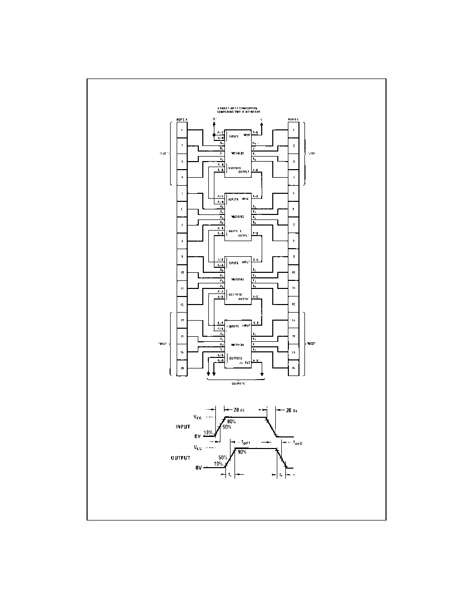
Typical Applications
Four Digit Comparator
Switching Time Waveforms
Unused inputs must be tied to an appropriate logic level.
5
www.fairchildsemi.com
MM74C85 4-Bi
t Magnit
ude C
o
m
p
ar
ator
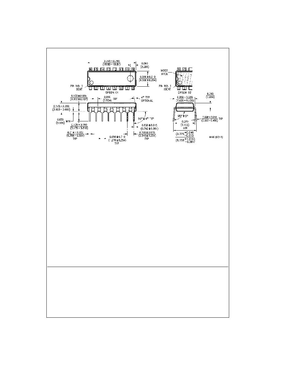
Physical Dimensions
inches (millimeters) unless otherwise noted
16-Lead Plastic Dual-In-Line Package (PDIP), JEDEC MS-001, 0.300" Wide
Package Number N16E
Fairchild does not assume any responsibility for use of any circuitry described, no circuit patent licenses are implied and
Fairchild reserves the right at any time without notice to change said circuitry and specifications.
LIFE SUPPORT POLICY
FAIRCHILD'S PRODUCTS ARE NOT AUTHORIZED FOR USE AS CRITICAL COMPONENTS IN LIFE SUPPORT
DEVICES OR SYSTEMS WITHOUT THE EXPRESS WRITTEN APPROVAL OF THE PRESIDENT OF FAIRCHILD
SEMICONDUCTOR CORPORATION. As used herein:
1. Life support devices or systems are devices or systems
which, (a) are intended for surgical implant into the
body, or (b) support or sustain life, and (c) whose failure
to perform when properly used in accordance with
instructions for use provided in the labeling, can be rea-
sonably expected to result in a significant injury to the
user.
2. A critical component in any component of a life support
device or system whose failure to perform can be rea-
sonably expected to cause the failure of the life support
device or system, or to affect its safety or effectiveness.
www.fairchildsemi.com