 | –≠–ª–µ–∫—Ç—Ä–æ–Ω–Ω—ã–π –∫–æ–º–ø–æ–Ω–µ–Ω—Ç: MM74C89 | –°–∫–∞—á–∞—Ç—å:  PDF PDF  ZIP ZIP |
October 1987
Revised January 1999
MM74C89 64-Bi
t 3-
S
T
A
T
E
Rand
om
Access Read/Wri
t
e Mem
o
r
y
© 1999 Fairchild Semiconductor Corporation
DS005888.prf
www.fairchildsemi.com
MM74C89
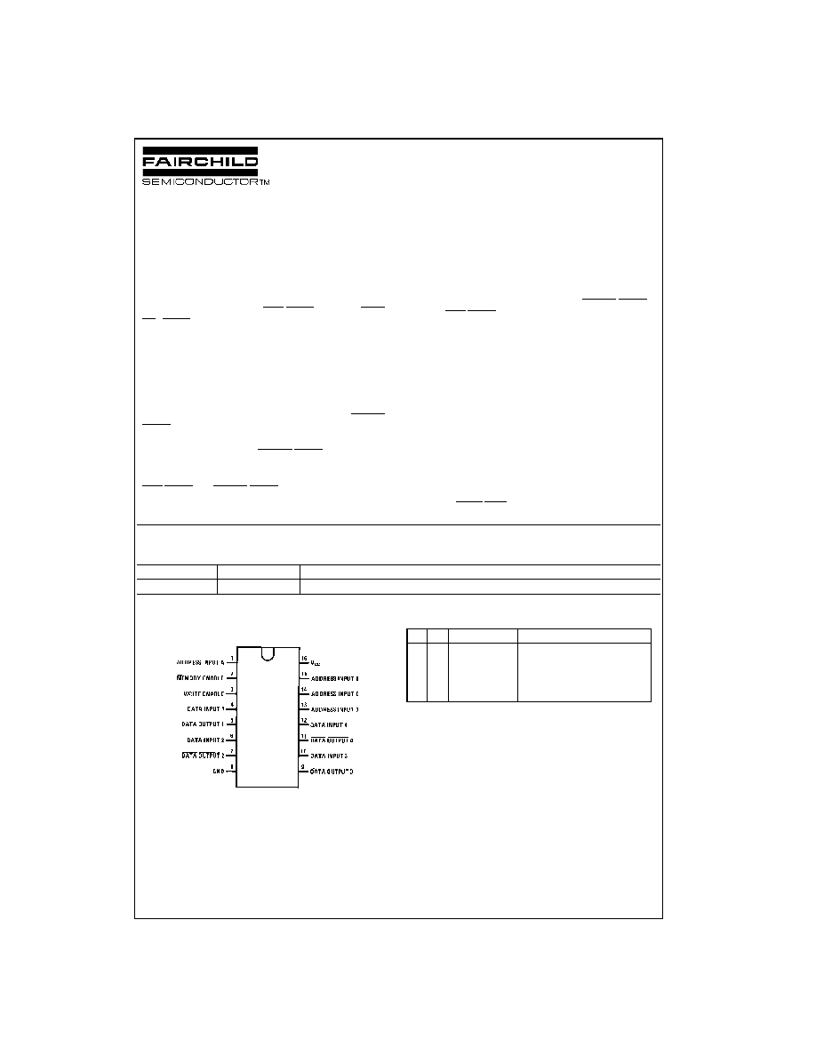
64-Bit 3-STATE Random Access Read/Write Memory
General Description
The MM74C89 is a 16-word by 4-bit random access read/
write memory. Inputs to the memory consist of four address
lines, four data input lines, a write enable line and a mem-
ory enable line. The four binary address inputs are
decoded internally to select each of the 16 possible word
locations. An internal address register latches the address
information on the positive to negative transition of the
memory enable input. The four 3-STATE data output lines
working in conjunction with the memory enable input pro-
vide for easy memory expansion.
Address Operation: Address inputs must be stable t
SA
prior to the positive to negative transition of memory
enable. It is thus not necessary to hold address information
stable for more than t
HA
after the memory is enabled (posi-
tive to negative transition of memory enable).
Write Operation: Information present at the data inputs is
written into the memory at the selected address by bringing
write enable and memory enable LOW.
Read Operation: The complement of the information
which was written into the memory is non-destructively
read out at the four outputs. This is accomplished by
selecting the desired address and bringing memory enable
LOW and write enable HIGH.
When the device is writing or disabled the output assumes
a 3-STATE (Hi-z) condition.
Features
s
Wide supply voltage range:
3.0V to 15V
s
Guaranteed noise margin:
1.0V
s
High noise immunity:
0.45 V
CC
(typ.)
s
Low power TTL compatibility:
fan out of 2 driving 74L
s
Low power consumption:
100 nW/package (typ.)
s
Fast access time:
130 ns (typ.) at V
CC
=
10V
s
3-STATE output
Note: The timing is different than the DM7489 in that a positive to negative
transition of the memory enable must occur for the memory to be selected.
Ordering Code:
Connection Diagram
Pin Assignments for DIP
Top View
Truth Table
Order Number
Package Number Package Description
MM74C89N
N16E
16-Lead Plastic Dual-In-Line Package (PDIP), JEDEC MS-001, 0.300" Wide
ME WE
Operation
Condition of Outputs
L
L
Write
3-STATE
L
H
Read
Complement of Selected Word
H
L
Inhibit, Storage 3-STATE
H
H
Inhibit, Storage 3-STATE
www.fairchildsemi.com
2
MM
74C89
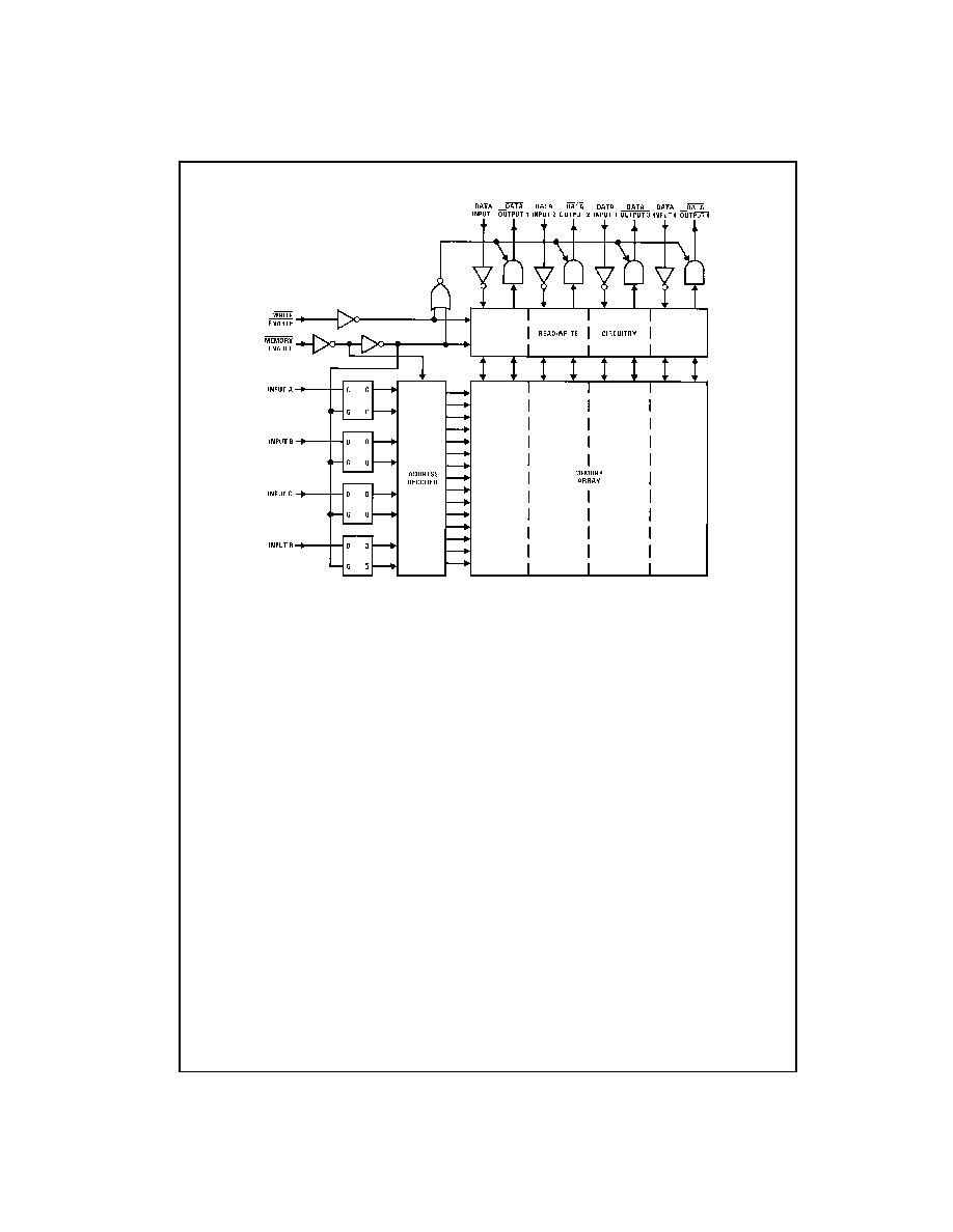
Logic Diagram
3
www.fairchildsemi.com
MM74C89
Absolute Maximum Ratings
(Note 1)
Note 1: "Absolute Maximum Ratings" are those values beyond which the
safety of the device cannot be guaranteed. Except for "Operating Range"
they are not meant to imply that the devices should be operated at these
limits. The table of "Electrical Characteristics" provides conditions for actual
device operation.
DC Electrical Characteristics
Min/Max limits apply across temperature range, unless otherwise noted
Voltage at any Pin
-
0.3V to V
CC
+
0.3V
Operating Temperature Range
-
40
∞
C to
+
85
∞
C
Storage Temperature Range (T
S
)
-
65
∞
C to
+
150
∞
C
Power Dissipation (P
D
)
Dual-In-Line
700 mW
Small Outline
500 mW
Operating V
CC
Range
3.0V to 15V
Absolute Maximum V
CC
18V
Lead Temperature (T
L
)
(Soldering, 10 seconds)
260
∞
C
Symbol
Parameter
Conditions
Min
Typ
Max
Units
CMOS TO CMOS
V
IN(1)
Logical "1" Input Voltage
V
CC
=
5.0V
3.5
V
V
CC
=
10V
8.0
V
V
IN(0)
Logical "0" Input Voltage
V
CC
=
5.0V
1.5
V
V
CC
=
10V
2.0
V
V
OUT(1)
Logical "1" Output Voltage
V
CC
=
5.0V, I
O
=
-
10
µ
A
4.5
V
V
CC
=
10V, I
O
=
-
10
µ
A
9.0
V
V
OUT(0)
Logical "0" Output Voltage
V
CC
=
5.0V, I
O
=
+
10
µ
A
0.5
V
V
CC
=
10V, I
O
=
+
10
µ
A
1.0
V
I
IN(1)
Logical "1" Input Current
V
CC
=
15V, V
IN
=
15V
-
0.005
1.0
µ
A
I
IN(0)
Logical "0" Input Current
V
CC
=
15V, V
IN
=
0V
-
1.0
-
0.005
µ
A
I
OZ
Output Current in High
V
CC
=
15V, V
=
15V
0.005
1.0
µ
A
Impedance State
V
CC
=
15V, V
O
=
0V
-
1.0
-
0.005
µ
A
I
CC
Supply Current
V
CC
=
15V
0.05
300
µ
A
CMOS/LPTTL INTERFACE
V
IN(1)
Logical "1" Input Voltage
V
CC
=
4.75V
V
CC
-
1.5
V
V
IN(0)
Logical "0" Input Voltage
V
CC
=
4.75V
0.8
V
V
OUT(1)
Logical "1" Output Voltage
V
CC
=
4.75V, I
O
=
-
360
µ
A
2.4
V
V
OUT(0)
Logical "0" Output Voltage
V
CC
=
4.75V, I
O
=
+
360
µ
A
0.4
V
OUTPUT DRIVE (See 54C/74C Family Characteristics Data Sheet) (Short Circuit Current)
I
SOURCE
Output Source Current
V
CC
=
5.0V, V
OUT
=
0V
-
1.75
-
3.3
mA
(P-Channel)
T
A
=
25
∞
C
I
SOURCE
Output Source Current
V
CC
=
10V, V
OUT
=
0V
-
8.0
-
15
mA
(P-Channel)
T
A
=
25
∞
C
I
SINK
Output Sink Current
V
CC
=
5.0V, V
OUT
=
V
CC
1.75
3.6
mA
(N-Channel)
T
A
=
25
∞
C
I
SINK
Output Sink Current
V
CC
=
10V, V
OUT
=
V
CC
8.0
16
mA
(N-Channel)
T
A
=
25
∞
C
www.fairchildsemi.com
4
MM
74C89
AC Electrical Characteristics
(Note 2)
T
A
=
25
∞
C, C
L
=
50 pF, unless otherwise noted
Note 2: AC Parameters are guaranteed by DC correlated testing.
Note 3: Capacitance is guaranteed by periodic testing.
Note 4: C
PD
determines the no load AC power consumption of any CMOS device. For complete explanation see Family Characteristics application note,
AN-90.
Symbol
Parameter
Conditions
Min
Typ
Max
Units
t
pd
Propagation Delay from
V
CC
=
5V
270
500
ns
Memory Enable
V
CC
=
10V
100
220
ns
t
ACC
Access Time from
V
CC
=
5V
350
650
ns
Address Input
V
CC
=
10V
130
280
ns
t
SA
Address Setup Time
V
CC
=
5V
150
ns
V
CC
=
10V
60
ns
t
HA
Address Hold Time
V
CC
=
5V
60
ns
V
CC
=
10V
40
ns
t
ME
Memory Enable Pulse Width
V
CC
=
5V
400
250
ns
V
CC
=
10V
150
90
ns
t
SR
Write Enable Setup
V
CC
=
5V
0
ns
Time for a Read
V
CC
=
10V
0
ns
t
WS
Write Enable Setup
V
CC
=
5V
t
ME
ns
Time for a Write
V
CC
=
10V
t
ME
ns
t
WE
Write Enable Pulse Width
V
CC
=
5V, t
WS
=
0
300
160
ns
V
CC
=
10V, t
WS
=
0
100
60
ns
t
HD
Data Input Hold Time
V
CC
=
5V
50
ns
V
CC
=
10V
25
ns
t
SD
Data Input Setup
V
CC
=
5V
50
ns
V
CC
=
10V
25
ns
t
1H
, t
0H
Propagation Delay from a Logical
V
CC
=
5V, C
L
=
5 pF, R
L
=
10k
180
300
ns
"1" or Logical "0" to the High
V
CC
=
10V, C
L
=
5 pF, R
L
=
10k
-
85
120
ns
Impedance State from
Memory Enable
t
1H
, t
0H
Propagation Delay from a Logical
V
CC
=
50V, C
L
=
5 pF, R
L
=
10k
180
300
ns
"1" or Logical "0" to the High
V
CC
=
10V, C
L
=
5 pF, R
L
=
10k
85
120
ns
Impedance State from
Write Enable
C
IN
Input Capacity
Any Input (Note 3)
5
pF
C
OUT
Output Capacity
Any Output (Note 3)
6.5
pF
C
PD
Power Dissipation Capacity
(Note 4)
230
pF
5
www.fairchildsemi.com
MM74C89
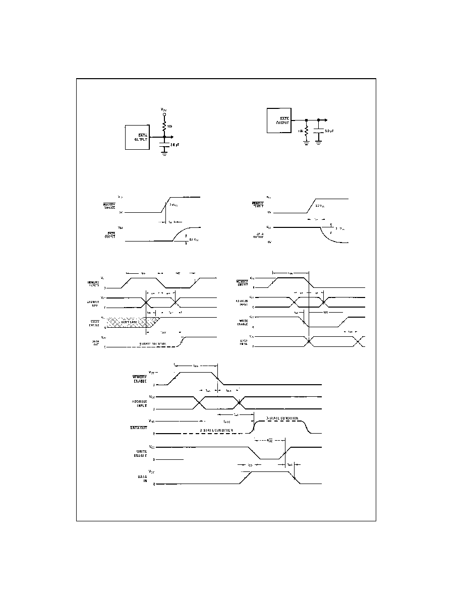
AC Test Circuits
t
0H
t
1H
Switching Time Waveforms
t
0H
t
1H
Read Cycle
Write Cycle
Read Modify Write Cycle
t
f
=
10 ns
t
r
=
60 ns