October 1987
Revised January 1999
MM74C912 6-Di
git
B
CD Displ
a
y
Cont
r
o
l
l
er
/Dr
i
ver
© 1999 Fairchild Semiconductor Corporation
DS005916.prf
www.fairchildsemi.com
MM74C912
6-Digit BCD Display Controller/Driver
General Description
The MM74C912 display controllers are interface elements,
with memory, that drive a 6-digit, 8-segment LED display.
The display controllers receive data information through 5
data inputs A, B, C, D and DP, and digit information through
3 address inputs K1, K2 and K3.
The input data is written into the register selected by the
address information when CHIP ENABLE, (CE), and
WRITE ENABLE, (WE), are LOW and is latched when
either CE or WE return HIGH. Data hold time is not
required. A self-contained internal oscillator sequentially
presents the stored data to a decoder where 4 data bits
control the format of the displayed character and 1 bit con-
trols the decimal point. The internal oscillator is controlled
by a control input labeled OSCILLATOR ENABLE, (OSE),
which is tied LOW in normal operation. A high level at OSE
prevents automatic refresh of the display.
The 7-segment plus decimal point output information
directly drives an LED display through high drive (100 mA
typ.) output drivers. The drivers are active when the control
pin labeled SEGMENT OUTPUT ENABLE, (SOE), is LOW
and go into 3-STATE when SOE is HIGH. This feature
allows for duty cycle brightness control and for disabling
the output drivers for power conservation.
The MM74C912 segment decoder converts BCD data into
7-segment format.
All inputs are TTL compatible and do not clamp to the V
CC
supply.
Features
s
Direct segment drive (100 mA typ.) 3-STATE
s
6 registers addressed like RAM
s
Internal oscillator and scanning circuit
s
Direct base drive to digit transistor (20 mA typ.)
s
Internal segment decoder
s
TTL compatible inputs
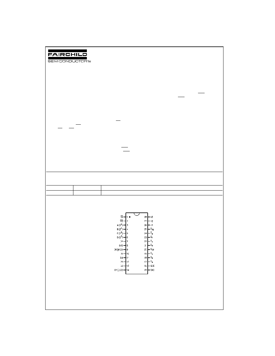
Ordering Code:
Connection Diagram
Dual-In-Line Package
Top View
Order Number
Package Number
Package Description
MM74C912N
N28B
28-Lead Plastic Dual-In-Line Package (PDIP), JEDEC MS-010, 0.600" Wide
3
www.fairchildsemi.com
MM74C912
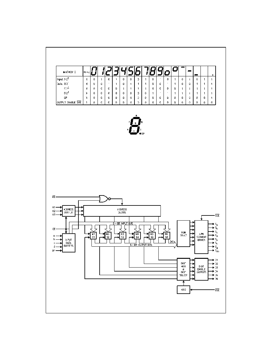
Functional Description
Character Font
Segment Identification
The MM74C912 display controller is manufactured using
metal gate CMOS technology. A single 5V 74 series TTL
supply can be used for power and should be bypassed at
the V
CC
pin.
All inputs are TTL compatible; the segment outputs drive
the LED display directly through current limiting resistors.
The digit outputs are designed to directly drive the base of
a grounded emitter digit transistor without the need of a
Darlington configuration.
As seen in the block diagram, these display controllers
contain six 5-bit registers; any one of which may be ran-
domly written. The internal multiplexer scans the registers
and refreshes the display. This combination of write only
memory and self-scan display makes the display controller
a "refreshing experience" for an over-burdened micropro-
cessor.
Block Diagram
www.fairchildsemi.com
4
M
M
74C912
Absolute Maximum Ratings
(Note 2)
(Note 3)
Note 2: "Absolute Maximum Ratings" are those values beyond which the
safety of the device cannot be guaranteed. Except for "Operating Range"
they are not meant to imply that the device should be operated at these lim-
its. The table of "Electrical Characteristics" provides conditions for actual
device operation.
Note 3: All voltages reference to ground.
DC Electrical Characteristics
Min/Max limits apply at 40
∞
C
T
J
85
∞
C, unless otherwise noted
Note 4:
JA
measured in free air with device soldered into printed circuit board.
Voltage at Any Pin
Except Inputs
-
0.3V to V
CC
+
0.3V
Voltage at Any Input
-
0.3V to
+
15V
Operating Temperature
Range (T
A
)
-
40
∞
C to
+
85
∞
C
Storage Temperature
Range (T
S
)
-
65
∞
C to
+
150
∞
C
Power Dissipation (P
D
)
Refer to P
D MAX
vs T
A
Graph
Operating V
CC
Range
3V to 6V
Absolute Maximum (V
CC
)
6.5V
Lead Temperature
(Soldering, 10 seconds)
260
∞
C
Symbol
Parameter
Conditions
Min
Typ
Max
Units
CMOS TO CMOS
V
IN(1)
Logical "1" Input Voltage
V
CC
=
5V
3.0
V
V
IN(0)
Logical "0" Input Voltage
V
CC
=
5V
1.5
V
I
IN(1)
Logical "1" Input Current
V
CC
=
5V, V
IN
=
15V
0.005
1.0
µ
A
I
IN(0)
Logical "0" Input Current
V
CC
=
5V, V
IN
=
0V
-
1.0
-
0.005
µ
A
I
CC
Supply Current
V
CC
=
5V, Outputs Open
0.5
2
mA
I
OUT
3-STATE
V
CC
=
5V, V
O
=
5V
0.03
10
µ
A
Output Current
V
CC
=
5V, V
O
=
0V
-
10
-
0.03
µ
A
CMOS/LPTTL INTERFACE
V
IN(1)
Logical "1" Input Voltage
V
CC
=
4.75V
V
CC
-
2.0
V
V
IN(0)
Logical "0" Input Voltage
V
CC
=
4.75V
0.8
V
OUTPUT DRIVE
I
SH
High Level
V
CC
=
5V, V
O
=
3.4V
Segment Current
T
J
=
25
∞
C
-
60
-
100
mA
T
J
=
100
∞
C
-
40
-
60
mA
I
DH
High Level
V
CC
=
5V, V
O
=
1V
Digit Current
T
J
=
25
∞
C
-
10
-
20
mA
T
J
=
100
∞
C
-
7
-
15
mA
V
OUT(1)
Logical "1" Output Voltage
V
CC
=
5V, I
O
=
-
360
µ
A
4.6
V
Any Digit
V
OUT(0)
Logical "0" Output Voltage
V
CC
=
5V, I
O
=
360
µ
A
0.4
V
Any Digit
JA
Thermal Resistance
(Note 4)
100
∞
C/W
5
www.fairchildsemi.com
MM74C912
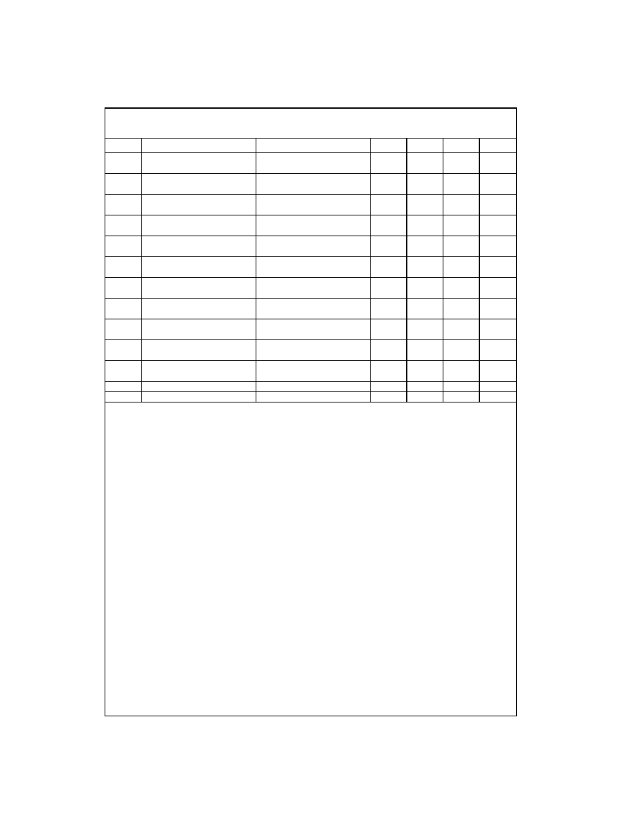
AC Electrical Characteristics
(Note 5)
V
CC
=
5V, t
r
=
t
f
=
20 ns, C
L
=
50 pF
Note 5: AC Parameters are guaranteed by DC correlated testing.
Note 6: Capacitance is guaranteed by periodic testing.
Symbol
Parameter
Conditions
Min
Typ
Max
Units
t
CW
Chip Enable to Write
T
J
=
25
∞
C
35
15
ns
Enable Setup Time
T
J
=
125
∞
C
50
20
ns
t
AW
Address to Write
T
J
=
25
∞
C
35
15
ns
Enable Setup Time
T
J
=
125
∞
C
50
20
ns
t
WW
Write Enable Width
T
J
=
25
∞
C
400
225
ns
T
J
=
125
∞
C
450
250
ns
t
DW
Data to Write Enable
T
J
=
25
∞
C
390
225
ns
Setup Time
T
J
=
125
∞
C
430
250
ns
t
WD
Write Enable to Data
T
J
=
25
∞
C
0
-
10
ns
Hold Time
T
J
=
125
∞
C
0
-
15
ns
t
WA
Write Enable to Address
T
J
=
25
∞
C
0
-
10
ns
Hold Time
T
J
=
125
∞
C
0
-
15
ns
t
WC
Write Enable to Chip Enable
T
J
=
25
∞
C
50
30
ns
Hold Time
T
J
=
125
∞
C
75
40
ns
t
1H
, t
0H
Logical "1", Logical "0"
R
L
=
10k, T
J
=
25
∞
C
275
500
ns
Levels into 3-STATE
C
L
=
10 pF, T
J
=
125
∞
C
325
600
ns
t
H1
, t
H0
3-STATE to Logical "1" to
R
L
=
10k, T
J
=
25
∞
C
325
600
ns
Logical "0" Level
C
L
=
50 pF, T
J
=
125
∞
C
375
700
ns
t
IB
Interdigit Blanking Time
T
J
=
25
∞
C
5
10
µ
s
T
J
=
125
∞
C
10
20
µ
s
f
MUX
Multiplex Scan Frequency
T
J
=
25
∞
C
350
Hz
T
J
=
125
∞
C
250
Hz
C
IN
Input Capacitance
(Note 6)
5
7.5
pF
C
OUT
3-STATE Output Capacitance
(Note 6)
30
50
pF