 | –≠–ª–µ–∫—Ç—Ä–æ–Ω–Ω—ã–π –∫–æ–º–ø–æ–Ω–µ–Ω—Ç: MM74C914M | –°–∫–∞—á–∞—Ç—å:  PDF PDF  ZIP ZIP |
October 1987
Revised January 1999
MM74C914 He
x Sc
hm
i
t
t
T
r
i
g
g
e
r wit
h
Ext
ended In
put V
o
lt
a
g
e
© 1999 Fairchild Semiconductor Corporation
DS005917.prf
www.fairchildsemi.com
MM74C914
Hex Schmitt Trigger with Extended Input Voltage
General Description
The MM74C914 is a monolithic CMOS Hex Schmitt trigger
with special input protection scheme. This scheme allows
the input voltage levels to exceed V
CC
or ground by at least
10V (V
CC
-
25V to GND
+
25V), and is valuable for applica-
tions involving voltage level shifting or mismatched power
supplies.
The positive and negative-going threshold voltages, V
T
+
and V
T
-
, show low variation with respect to temperature
(typ 0.0005V/
∞
C at V
CC
=
10V). And the hysteresis, V
T
+
-
V
T
-
0.2 V
CC
is guaranteed.
Features
s
Hysteresis:
0.45 V
CC
(typ.) 0.2 V
CC
guaranteed
s
Special input protection:
Extended Input Voltage
Range
s
Wide supply voltage range:
3V to 15V
s
High noise immunity:
0.7 V
CC
(typ.)
s
Low power TTL compatibility:
Fan out of 2 driving 74L
Ordering Code:
Device also available in Tape and Reel. Specify by appending suffix letter "X" to the ordering code.
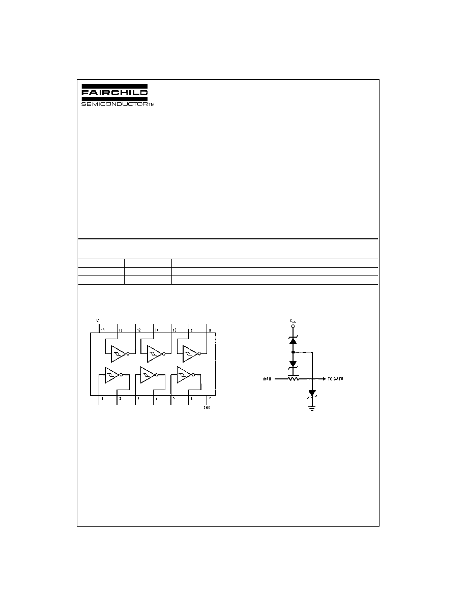
Connection Diagrams
Pin Assignments for DIP
Top View
Special Input Protection
8V
25V
for the diodes.
Order Number
Package Number
Package Description
MM74C914M
M14A
14-Lead Small Outline Integrated Circuit (SOIC), JEDEC MS-120, 0.150" Narrow
MM74C914N
N14A
14-Lead Plastic Dual-In-Line Package (PDIP), JEDEC MS-001, 0.300" Wide
www.fairchildsemi.com
2
M
M
74C914
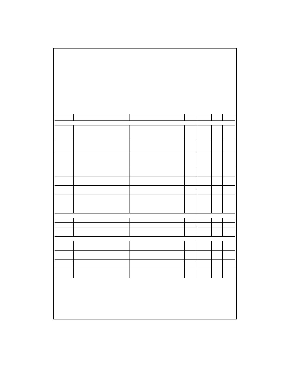
Absolute Maximum Ratings
(Note 1)
Note 1: "Absolute Maximum Ratings" are those values beyond which the
safety of the device cannot be guaranteed. Except for "Operating Tempera-
ture Range", they are not meant to imply that the devices should be oper-
ated at these limits. The Electrical Characteristics tables provide conditions
for actual device operation.
DC Electrical Characteristics
Min/Max limits apply across temperature range unless otherwise noted
Note 2: Only one input is at Ω V
CC
, the others are either at V
CC
or GND.
Voltage at any Input Pin
V
CC
-
25V to GND
+
25V
Voltage at any other Pin
-
0.3Vto V
CC
+
0.3V
Operating Temperature Range (T
A
)
-
40
∞
C to
+
85
∞
C
Storage Temperature Range (T
S
)
-
65
∞
C to
+
150
∞
C
Power Dissipation
Dual-In-Line
700 mW
Small Outline
500mW
Operating V
CC
Range
3V to 15V
Absolute Maximum (V
CC
)
18V
Lead Temperature (T
L
)
(Soldering, 10 seconds)
300
∞
C
Symbol
Parameter
Conditions
Min
Typ
Max
Units
CMOS TO CMOS
V
T
+
Positive Going Threshold Voltage
V
CC
=
5V
3.0
3.6
4.3
V
V
CC
=
10V
6.0
6.8
8.6
V
V
CC
=
15V
9.0
10
12.9
V
T
-
Negative Going Threshold Voltage
V
CC
=
5V
0.7
1.4
2.0
V
V
CC
=
10V
1.4
3.2
4.0
V
V
CC
=
15V
2.1
5
6.0
V
T
+
-
V
T
-
Hysteresis
V
CC
=
5V
1.0
2.2
3.6
V
V
CC
=
10V
2.0
3.6
7.2
V
V
CC
=
15V
3.0
5
10.8
V
V
OUT(1)
Logical"1" Output Voltage
V
CC
=
5V, I
O
=
-
10
µ
A
4.5
V
V
CC
=
10V, I
O
=
-
10
µ
A
9.0
V
V
OUT(0)
Logical "0" Output Voltage
V
CC
=
5V, I
O
=
+
10
µ
A
0.5
V
V
CC
=
10V, I
O
=
+
10
µ
A
1.0
V
I
IN(1)
Logical "1" Input Current
V
CC
=
15V, V
IN
=
25V
0.005
5.0
µ
A
I
IN(0)
Logical "0" Input Current
V
CC
=
15V, V
IN
=
-
10V
-
100
-
0.005
µ
A
I
CC
Supply Current
V
CC
=
15V, V
IN
=
-
10V/25V
0.05
300
µ
A
V
CC
=
5V, V
IN
=
-
2.5V (Note 2)
20
µ
A
V
CC
=
10V, V
IN
=
5V (Note 2)
200
µ
A
V
CC
=
15V, V
IN
=
7.5V (Note 2)
600
µ
A
CMOS/LPTTL INTERFACE
V
IN(1)
Logical "1" Input Voltage
V
CC
=
5V
4.3
V
V
IN(0)
Logical "0" Input Voltage
V
CC
=
5V
0.7
V
V
OUT(1)
Logical "1" Output Voltage
V
CC
=
4.75V, I
O
=
-
360
µ
A
2.4
V
V
OUT(0)
Logical "0" Output Voltage
V
CC
=
4.75V, I
O
=
360
µ
A
0.4
V
OUTPUT DRIVE (See Family Characteristics Data Sheet) (Short Circuit Current)
I
SOURCE
Output Source Current
V
CC
=
5V, V
OUT
=
0V, T
A
=
25
∞
C
-
1.75
-
3.3
mA
(P-Channel)
I
SOURCE
Output Source Current
V
CC
=
10V, V
OUT
=
0V, T
A
=
25
∞
C
-
8.0
-
15
mA
(P-Channel)
I
SINK
Output Sink Current
V
CC
=
5V, V
OUT
=
V
CC
, T
A
=
25
∞
C
1.75
3.6
mA
(N-Channel)
I
SINK
Output Sink Current
V
CC
=
10V, V
OUT
=
V
CC
, T
A
=
25
∞
C
8.0
16
mA
(N-Channel)
3
www.fairchildsemi.com
MM74C914
AC Electrical Characteristics
(Note 3)
T
A
=
25
∞
C, C
L
=
50 pF, unless otherwise specified
Note 3: AC Parameters are guaranteed by DC correlated testing.
Note 4: Capacitance is guaranteed by periodic testing.
Note 5: C
PD
determines the no load AC power consumption of any CMOS device. For complete explanation see Family Characteristics Application Note,
AN-90.
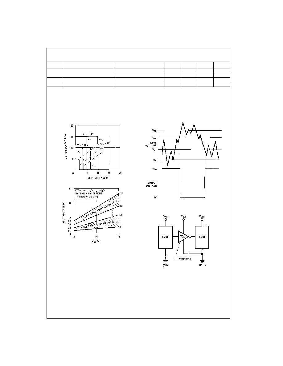
Typical Performance Characteristics
Typical Transfer Characteristics
Guaranteed Trip Point Range
Typical Application
Note: V
CC1
=
V
CC2
GND1
=
GND2
Symbol
Parameter
Conditions
Min
Typ
Max
Units
t
PHL
Propagation Delay from Input to Output
V
CC
=
5V
220
400
ns
t
PLH
V
CC
=
10V
80
200
ns
C
IN
Input Capacitance
Any Input (Note 4)
5
pF
C
PD
Power Dissipation Capacitance
Per Gate (Note 5)
20
pF
www.fairchildsemi.com
4
M
M
74C914
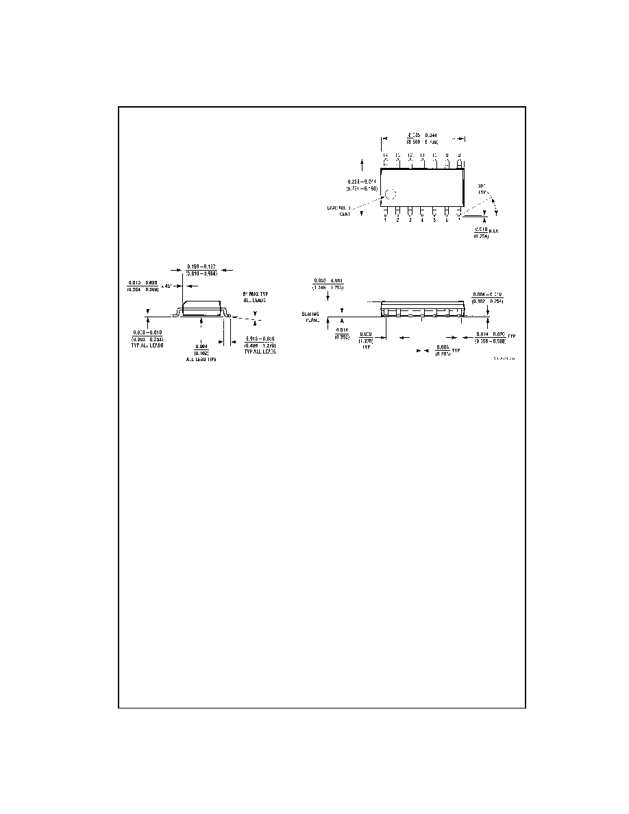
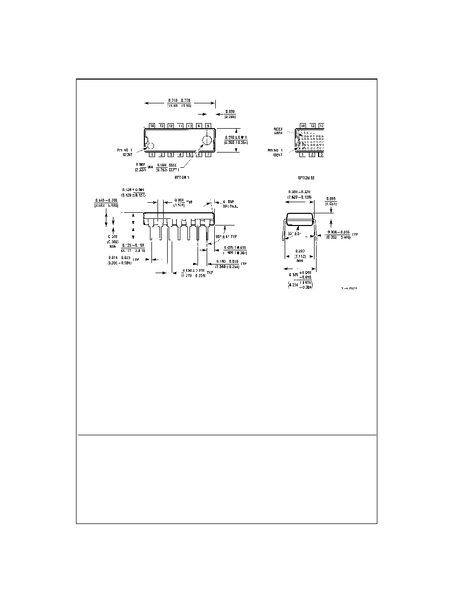
Physical Dimensions
inches (millimeters) unless otherwise noted
14-Lead Small Outline Integrated Circuit (SOIC), JEDEC MS-120, 0.150" Narrow
Package Number M14A
Fairchild does not assume any responsibility for use of any circuitry described, no circuit patent licenses are implied and Fairchild reserves the right at any time without notice to change said circuitry and specifications.
MM74C914 He
x Sc
hm
i
t
t
T
r
i
g
g
e
r wit
h
Ext
ended In
put V
o
lt
a
g
e
LIFE SUPPORT POLICY
FAIRCHILD'S PRODUCTS ARE NOT AUTHORIZED FOR USE AS CRITICAL COMPONENTS IN LIFE SUPPORT
DEVICES OR SYSTEMS WITHOUT THE EXPRESS WRITTEN APPROVAL OF THE PRESIDENT OF FAIRCHILD
SEMICONDUCTOR CORPORATION. As used herein:
1. Life support devices or systems are devices or systems
which, (a) are intended for surgical implant into the
body, or (b) support or sustain life, and (c) whose failure
to perform when properly used in accordance with
instructions for use provided in the labeling, can be rea-
sonably expected to result in a significant injury to the
user.
2. A critical component in any component of a life support
device or system whose failure to perform can be rea-
sonably expected to cause the failure of the life support
device or system, or to affect its safety or effectiveness.
www.fairchildsemi.com
Physical Dimensions
inches (millimeters) unless otherwise noted (Continued)
14-Lead Plastic Dual-In-Line Package (PDIP), JEDEC MS-001, 0.300" Wide
Package Number N14A