 | –≠–ª–µ–∫—Ç—Ä–æ–Ω–Ω—ã–π –∫–æ–º–ø–æ–Ω–µ–Ω—Ç: MM74C93 | –°–∫–∞—á–∞—Ç—å:  PDF PDF  ZIP ZIP |
© 2004 Fairchild Semiconductor Corporation
DS005889
www.fairchildsemi.com
October 1987
Revised January 2004
MM74C93 4-Bi
t Binar
y
Coun
ter
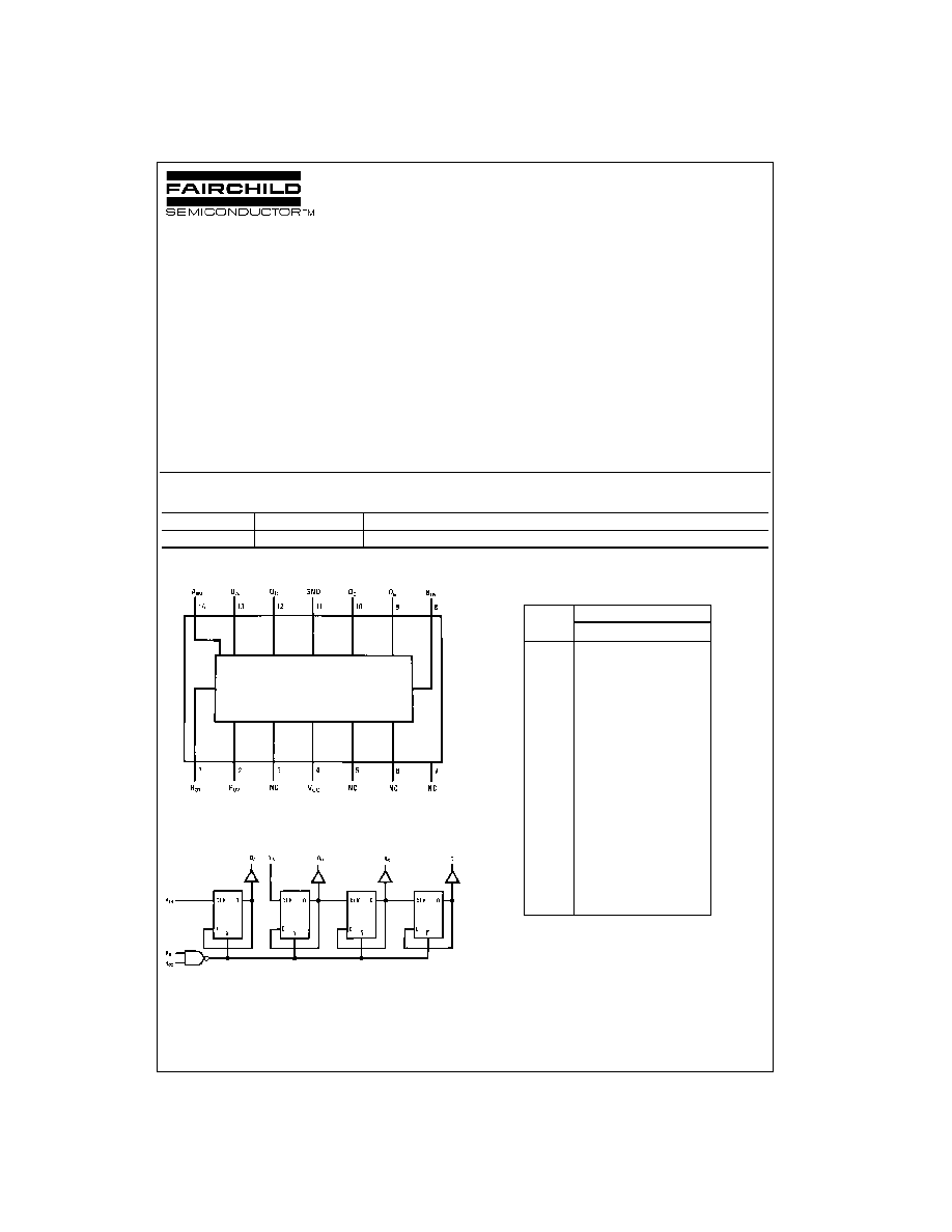
MM74C93
4-Bit Binary Counter
General Description
The MM74C93 binary counter and complementary MOS
(CMOS) integrated circuits constructed with N- and P-
channel enhancement mode transistors. The 4-bit binary
counter can be reset to zero by applying high logic level on
inputs R
01
and R
02
, and a separate flip-flop on the A-bit
enables the user to operate it as a divide-by-2, -8, or -16
divider. Counting occurs on the negative going edge of the
input pulse.
All inputs are protected against static discharge damage.
Features
s
Wide supply voltage range:
3V to 15V
s
Guaranteed noise margin:
1V
s
High noise immunity:
0.45 V
CC
(typ.)
s
Low power compatibility:
Fan out of 2 TTL driving 74L
s
The MM74C93 follows the MM74L93 Pinout
Ordering Code:
Connection Diagram
Top View
Logic Diagram
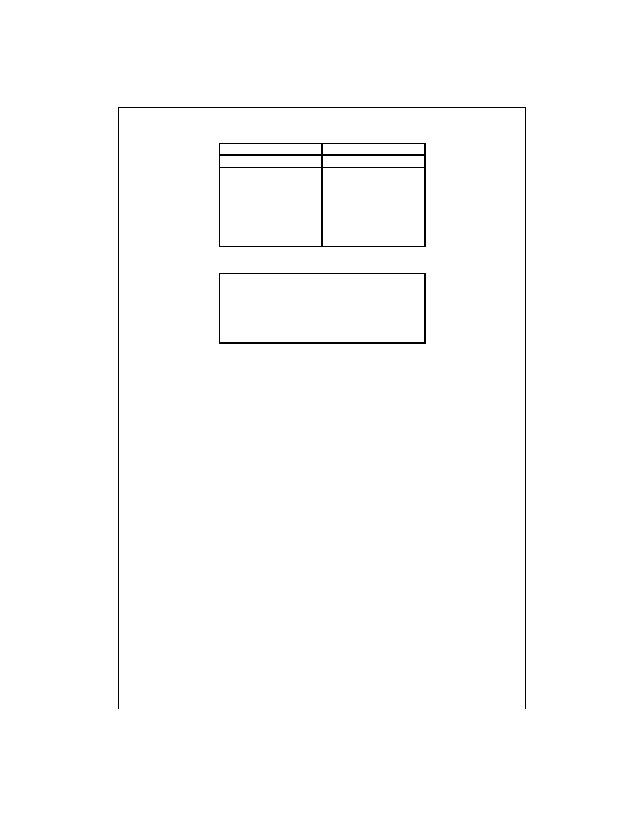
Truth Table
4-Bit Binary Counter Binary Count Sequence
Output Q
A
is connected to input B for binary count sequence.
H
=
HIGH Level
L
=
LOW Level
X
=
Irrelevant
Order Number
Package Number
Package Description
MM74C93N
N14A
14-Lead Plastic Dual-In-Line Package (PDIP), JEDEC MS-001, 0.300" Wide
Count
Output
Q
D
Q
C
Q
B
Q
A
0
L
L
L
L
1
L
L
L
H
2
L
L
H
L
3
L
L
H
H
4
L
H
L
L
5
L
H
L
H
6
L
H
H
L
7
L
H
H
H
8
H
L
L
L
9
H
L
L
H
10
H
L
H
L
11
H
L
H
H
12
H
H
L
L
13
H
H
L
H
14
H
H
H
L
15
H
H
H
H
www.fairchildsemi.com
2
MM
74C93
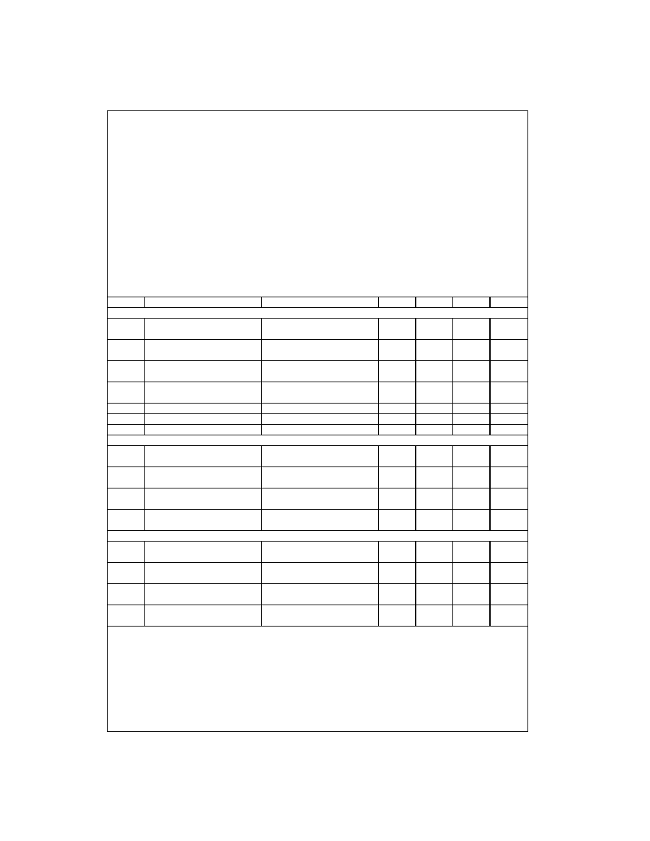
Function Tables
Reset/Count Function Table
Reset/Count Function Table
Reset Inputs
Output
R
01
R
02
R
91
R
92
Q
D
Q
C
Q
B
Q
A
H
H
L
X
L
L
L
L
H
H
X
L
L
L
L
L
X
X
H
H
H
L
L
H
X
L
X
L
Count
L
X
L
X
Count
L
X
X
L
Count
X
L
L
X
Count
Reset
Output
Inputs
R
01
R
02
Q
D
Q
C
Q
B
Q
A
H
H
L
L
L
L
L
X
Count
X
L
Count
3
www.fairchildsemi.com
MM74C93
Absolute Maximum Ratings
(Note 1)
Note 1: "Absolute Maximum Ratings" are those values beyond which the
safety of the device cannot be guaranteed. Except for "Operating Tempera-
ture Range", they are not meant to imply that the devices should be oper-
ated at these limits. The table of "Electrical Characteristics" provides
conditions for actual device operation.
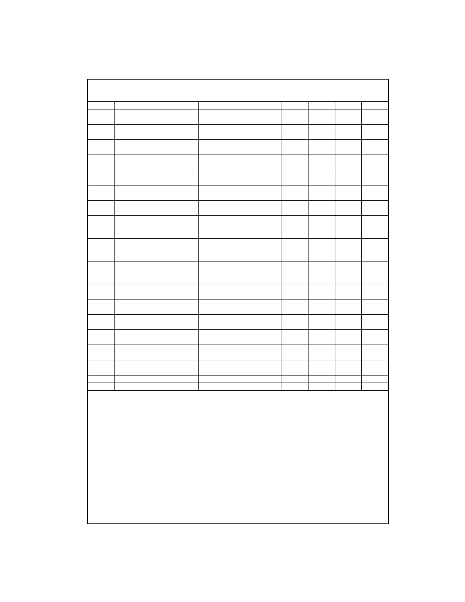
DC Electrical Characteristics
Min/Max limits apply across temperature range unless otherwise noted
Voltage at Any Pin (Note 1)
-
0.3V to V
CC
+
0.3V
Operating Temperature Range (T
A
)
-
55
∞
C to
+
125
∞
C
Power Dissipation (P
D
)
Dual-In-Line
700 mW
Small Outline
500 mW
Operating V
CC
Range
3V to 15V
Absolute Maximum V
CC
18V
Storage Temperature Range (T
S
)
-
65
∞
C to
+
150
∞
C
Lead Temperature (T
L
)
(Soldering, 10 seconds)
260
∞
C
Symbol
Parameter
Conditions
Min
Typ
Max
Units
CMOS TO CMOS
V
IN(1)
Logical "1" Input Voltage
V
CC
=
5V
3.5
V
V
CC
=
10V
8.0
V
IN(0)
Logical "0" Input Voltage
V
CC
=
5V
1.5
V
V
CC
=
10V
2.0
V
OUT(1)
Logical "1" Output Voltage
V
CC
=
5V, I
O
=
-
10
µ
A
4.5
V
V
CC
=
10V, I
O
=
-
10
µ
A
9.0
V
OUT(0)
Logical "0" Output Voltage
V
CC
=
5V, I
O
=
+
10
µ
A
0.5
V
V
CC
=
10V, I
O
=
+
10
µ
A
1.0
I
IN(1)
Logical "1" Input Current
V
CC
=
15V, V
IN
=
15V
0.005
1.0
µ
A
I
IN(0)
Logical "0" Input Current
V
CC
=
15V, V
IN
=
0V
-
1.0
-
0.005
µ
A
I
CC
Supply Current
V
CC
=
15V
0.05
300
µ
A
CMOS/LPTTL INTERFACE
V
IN(1)
Logical "1" Input Voltage
MM74C90, MM74C93
V
CC
=
4.75V
V
CC
-
1.5
V
V
IN(0)
Logical "0" Input Voltage
MM74C90, MM74C93
V
CC
=
4.75V
0.8
V
V
OUT(1)
Logical "1" Output Voltage
MM74C90, MM74C93
V
CC
=
4.75V, I
O
=
-
360
µ
A
2.4
V
V
OUT(0)
Logical "0" Output Voltage
MM74C90, MM74C93
V
CC
=
4.75V, I
O
=
-
360
µ
A
0.4
V
OUTPUT DRIVE (See Family Characteristics Data Sheet) (Short Circuit Current)
I
SOURCE
Output Source Current
V
CC
=
5V, V
OUT
=
0V
-
1.75
-
3.3
mA
(P-Channel)
T
A
=
25
∞
C
I
SOURCE
Output Source Current
V
CC
=
10V, V
OUT
=
0V
-
8.0
-
15
mA
(P-Channel)
T
A
=
25
∞
C
I
SINK
Output Sink Current
V
CC
=
5V, V
OUT
=
V
CC
1.75
3.6
mA
(N-Channel)
T
A
=
25
∞
C
I
SINK
Output Sink Current
V
CC
=
10V, V
OUT
=
V
CC
8.0
16
mA
(N-Channel)
T
A
=
25
∞
C
www.fairchildsemi.com
4
MM
74C93
AC Electrical Characteristics
(Note 2)
T
A
=
25
∞
C, C
L
=
50 pF, unless otherwise specified
Note 2: AC Parameters are guaranteed by DC correlated testing.
Note 3: Capacitance is guaranteed by periodic testing.
Note 4: C
PD
determines the no load ac power consumption of any CMOS device. For complete explanation see Family Characteristics application note--
AN-90.
Symbol
Parameter
Conditions
Min
Typ
Max
Units
t
pd0
, t
pd1
Propagation Delay Time
V
CC
=
5V
200
400
ns
from A
IN
to Q
A
V
CC
=
10
80
150
t
pd0
, t
pd1
Propagation Delay Time from
V
CC
=
5V
450
850
ns
A
IN
to Q
B
(MM74C93)
V
CC
=
10V
160
300
t
pd0
, t
pd1
Propagation Delay Time from
V
CC
=
5V
450
800
ns
A
IN
to Q
B
(MM74C90)
V
CC
=
10V
160
300
t
pd0
, t
pd1
Propagation Delay Time
V
CC
=
5V
500
1050
ns
from A
IN
to Q
C
(MM74C93)
V
CC
=
10
200
400
t
pd0
, t
pd1
Propagation Delay Time from
V
CC
=
5V
500
1000
ns
A
IN
to Q
C
(MM74C93)
V
CC
=
10V
200
400
t
pd0
, t
pd1
Propagation Delay Time from
V
CC
=
5V
600
1200
ns
A
IN
to Q
D
(MM74C93)
V
CC
=
10V
250
500
t
pd0
, t
pd1
Propagation Delay Time from
V
CC
=
5V
450
800
ns
A
IN
to Q
D
(MM74C90)
V
CC
=
10V
160
300
t
pd0
, t
pd1
Propagation Delay Time from
V
CC
=
5V
150
300
ns
R
01
or R
02
to Q
A
, Q
B
, Q
C
or Q
D
V
CC
=
10V
75
150
(MM74C93)
t
pd0
, t
pd1
Propagation Delay Time from
V
CC
=
5V
200
400
ns
R
01
or R
02
to Q
A
, Q
B
, Q
C
or Q
D
V
CC
=
10V
75
150
(MM74C90)
t
pd0
, t
pd1
Propagation Delay Time from
V
CC
=
5V
250
500
ns
R
91
or R
92
to Q
A
or Q
D
V
CC
=
10V
100
200
(MM74C90)
t
PW
Min. R
01
or R
02
Pulse Width
V
CC
=
5V
600
250
ns
(MM74C93)
V
CC
=
10V
30
125
t
PW
Min. R
01
or R
02
Pulse Width
V
CC
=
5V
600
250
ns
(MM74C90)
V
CC
=
10V
300
125
t
PW
Min. R
91
or R
92
Pulse Width
V
CC
=
5V
500
200
ns
(MM74C90)
V
CC
=
10V
250
100
t
r
, t
f
Maximum Clock Rise
V
CC
=
10V
15
µ
s
and Fall Time
V
CC
=
10V
5
t
W
Minimum Clock Pulse Width
V
CC
=
5V
250
100
ns
V
CC
=
10V
100
50
f
MAX
Maximum Clock Frequency
V
CC
=
5V
2
MHz
V
CC
=
10V
5
C
IN
Input Capacitance
Any Input (Note 3)
5
pF
C
PD
Power Dissipation Capacitance
Per Package (Note 4)
45
pF
5
www.fairchildsemi.com
MM74C93
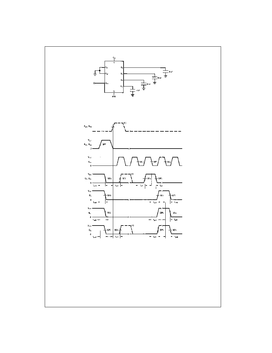
AC Test Circuits
Clock rise and fall time t
r
=
t
f
=
20 ns
Switching Time Waveforms
MM74C90 and MM74C93 are solid line waveforms. Dashed line waveforms are for MM74C90 only.