© 2005 Fairchild Semiconductor Corporation
DS005165
www.fairchildsemi.com
September 1983
Revised May 2005
MM74HC245A O
c
t
a
l 3-ST
A
T
E
T
r
anscei
ver
MM74HC245A
Octal 3-STATE Transceiver
General Description
The MM74HC245A 3-STATE bidirectional buffer utilizes
advanced silicon-gate CMOS technology, and is intended
for two-way asynchronous communication between data
buses. It has high drive current outputs which enable high
speed operation even when driving large bus capaci-
tances. This circuit possesses the low power consumption
and high noise immunity usually associated with CMOS cir-
cuitry, yet has speeds comparable to low power Schottky
TTL circuits.
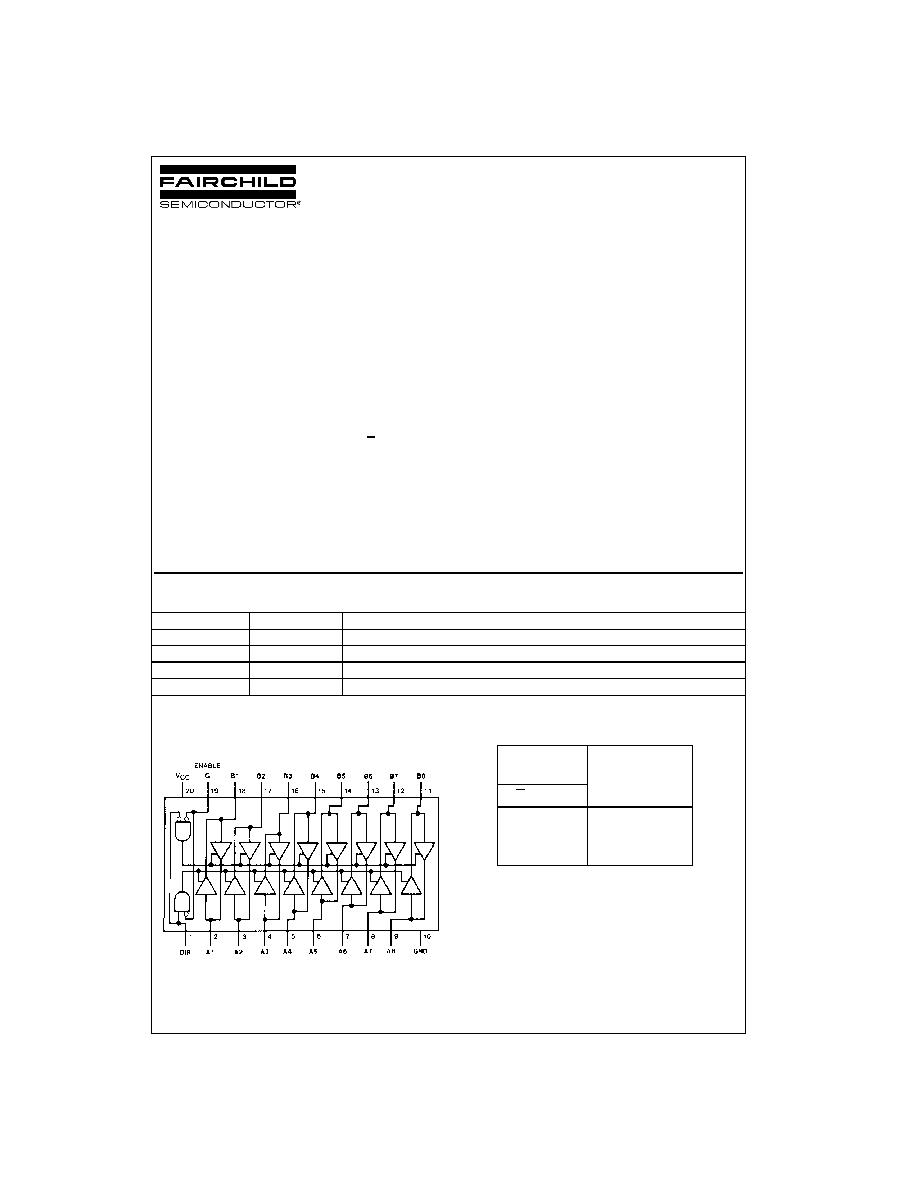
This device has an active LOW enable input G and a direc-
tion control input, DIR. When DIR is HIGH, data flows from
the A inputs to the B outputs. When DIR is LOW, data flows
from the B inputs to the A outputs. The MM74HC245A
transfers true data from one bus to the other.
This device can drive up to 15 LS-TTL Loads, and does not
have Schmitt trigger inputs. All inputs are protected from
damage due to static discharge by diodes to V
CC
and
ground.
Features
s
Typical propagation delay: 13 ns
s
Wide power supply range: 2≠6V
s
Low quiescent current: 80
P
A maximum (74 HC)
s
3-STATE outputs for connection to bus oriented systems
s
High output drive: 6 mA (minimum)
s
Same as the 645
Ordering Code:
Devices also available in Tape and Reel. Specify by appending the suffix letter "X" to the ordering code.
Connection Diagram
Pin Assignments for DIP, SOIC, SOP and TSSOP
Top View
Truth Table
H
HIGH Level
L
LOW Level
X
Irrelevant
Order Number
Package Number
Package Description
MM74HC245AWM
M20B
20-Lead Small Outline Integrated Circuit (SOIC), JEDEC MS-013, 0.300" Wide
MM74HC245ASJ
M20D
20-Lead Small Outline Package (SOP), EIAJ TYPE II, 5.3mm Wide
MM74HC245AMTC
MTC20
20-Lead Thin Shrink Small Outline Package (TSSOP), JEDEC MO-153, 4.4mm Wide
MM74HC245AN
N20A
20-Lead Plastic Dual-In-Line Package (PDIP), JEDEC MS-001, 0.300" Wide
Control
Inputs
Operation
G
DIR
L
L
B data to A bus
L
H
A data to B bus
H
X
Isolation
www.fairchildsemi.com
2
MM
74
H
C
24
5A
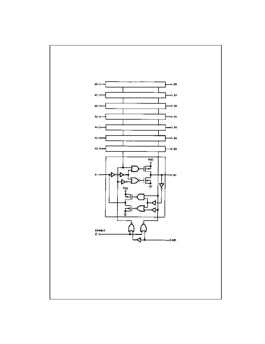
Logic Diagram

3
www.fairchildsemi.com
MM74HC245A
Absolute Maximum Ratings
(Note 1)
(Note 2)
Recommended Operating
Conditions
Note 1: Maximum Ratings are those values beyond which damage to the
device may occur.
Note 2: Unless otherwise specified all voltages are referenced to ground.
Note 3: Power Dissipation temperature derating -- plastic "N" package:
12 mW/
q
C from 65
q
C to 85
q
C.
DC Electrical Characteristics
(Note 4)
Note 4: For a power supply of 5V
r
10% the worst case output voltages (V
OH
, and V
OL
) occur for HC at 4.5V. Thus the 4.5V values should be used when
designing with this supply. Worst case V
IH
and V
IL
occur at V
CC
5.5V and 4.5V respectively. (The V
IH
value at 5.5V is 3.85V.) The worst case leakage cur-
rent (I
IN
, I
CC
, and I
OZ
) occur for CMOS at the higher voltage and so the 6.0V values should be used.
Supply Voltage (V
CC
)
0.5 to
7.0V
DC Input Voltage DIR and G pins (V
IN
)
1.5 to V
CC
1.5V
DC Input/Output Voltage (V
IN
, V
OUT
)
0.5 to V
CC
0.5V
Clamp Diode Current (I
CD
)
r
20 mA
DC Output Current, per pin (I
OUT
)
r
35 mA
DC V
CC
or GND Current, per pin (I
CC
)
r
70 mA
Storage Temperature Range (T
STG
)
65
q
C to
150
q
C
Power Dissipation (P
D
)
(Note 3)
600 mW
S.O. Package only
500 mW
Lead Temperature (T
L
)
(Soldering 10 seconds)
260
q
C
Min
Max
Units
Supply Voltage (V
CC
)
2
6
V
DC Input or Output Voltage
(V
IN
, V
OUT
)
0
V
CC
V
Operating Temperature Range (T
A
)
40
85
q
C
Input Rise/Fall Times
(t
r
, t
f
)
V
CC
2.0V
1000
ns
V
CC
4.5V
500
ns
V
CC
6.0V
400
ns
Symbol
Parameter
Conditions
V
CC
T
A
25
q
C
T
A
40 to 85
q
C T
A
55 to 125
q
C
Units
Typ
Guaranteed Limits
V
IH
Minimum HIGH Level Input
2.0V
1.5
1.5
1.5
V
Voltage
4.5V
3.15
3.15
3.15
V
6.0V
4.2
4.2
4.2
V
V
IL
Maximum LOW Level Input
2.0V
0.5
0.5
0.5
V
Voltage 4.5V
1.35
1.35
1.35
V
6.0V
1.8
1.8
1.8
V
V
OH
Minimum HIGH Level Output
V
IN
V
IH
or V
IL
Voltage
|I
OUT
|
d
20
P
A
2.0V
2.0
1.9
1.9
1.9
V
4.5V
4.5
4.4
4.4
4.4
V
6.0V
6.0
5.9
5.9
5.9
V
V
IN
V
IH
or V
IL
|I
OUT
|
d
6.0 mA
4.5V
4.2
3.98
3.84
3.7
V
|I
OUT
|
d
7.8 mA
6.0V
5.7
5.48
5.34
5.2
V
V
OL
Maximum LOW Level Output
V
IN
V
IH
or V
IL
Voltage
|I
OUT
|
d
20
P
A
2.0V
0
0.1
0.1
0.1
V
4.5V
0
0.1
0.1
0.1
V
6.0V
0
0.1
0.1
0.1
V
V
IN
V
IH
or V
IL
|I
OUT
|
d
6.0 mA
4.5V
0.2
0.26
0.33
0.4
V
|I
OUT
|
d
7.8 mA
6.0V
0.2
0.26
0.33
0.4
V
I
IN
Input Leakage
V
IN
V
CC
to GND
6.0V
r
0.1
r
1.0
r
1.0
P
A
Current (G and DIR)
I
OZ
Maximum 3-STATE Output
V
OUT
V
CC
or GND
6.0V
r
0.5
r
5.0
r
10
P
A
Leakage Current
Enable G
V
IH
I
CC
Maximum Quiescent Supply
V
IN
V
CC
or GND
6.0V
8.0
80
160
P
A
Current
I
OUT
0
P
A
www.fairchildsemi.com
4
MM
74
H
C
24
5A
AC Electrical Characteristics
V
CC
5V, T
A
25
q
C, t
r
t
f
6ns
AC Electrical Characteristics
V
CC
2.0V to 6.0V, C
L
50 pF, t
r
t
f
6ns (unless otherwise specified)
Note 5: C
PD
determines the no load dynamic power consumption, P
D
C
PD
V
CC
2
f
I
CC
V
CC
, and the no load dynamic current consumption, I
S
C
PD
V
CC
f
I
CC
.
Symbol
Parameter
Conditions
Typ
Guaranteed
Units
Limit
t
PHL
, t
PLH
Maximum Propagation Delay
C
L
45 pF
12
17
ns
t
PZH
, t
PZL
Maximum Output Enable
R
L
1 k
:
24
35
ns
Time
C
L
45 pF
t
PHZ
, t
PLZ
Maximum Output Disable
R
L
1 k
:
18
25
ns
Time
C
L
5 pF
Symbol
Parameter
Conditions
V
CC
T
A
25
q
C
T
A
40 to 85
q
C T
A
55 to 125
q
C
Units
Typ
Guaranteed Limits
t
PHL
,
Maximum Propagation
C
L
50 pF
2.0V
31
90
113
135
ns
t
PLH
Delay
C
L
150 pF
2.0V
41
96
116
128
ns
C
L
50 pF
4.5V
13
18
23
27
ns
C
L
150 pF
4.5V
17
22
28
33
ns
C
L
50 pF
6.0V
11
15
19
23
ns
C
L
150 pF
6.0V
14
19
23
28
ns
t
PZH
,
Maximum Output Enable
R
L
1 k
:
t
PZL
Time
C
L
50 pF
2.0V
71
190
240
285
ns
C
L
150 pF
2.0V
81
240
300
360
ns
C
L
50 pF
4.5V
26
38
48
57
ns
C
L
150 pF
4.5V
31
48
60
72
ns
C
L
50 pF
6.0V
21
32
41
48
ns
C
L
150 pF
6.0V
25
41
51
61
ns
t
PHZ
,
Maximum Output Disable
R
L
1 k
:
2.0V
39
135
169
203
ns
t
PLZ
Time
C
L
50 pF
4.5V
20
27
34
41
ns
6.0V
18
23
29
34
ns
t
TLH
, t
THL
Output Rise and Fall Time
C
L
50 pF
2.0V
20
60
75
90
ns
4.5V
6
12
15
18
ns
6.0V
5
10
13
15
ns
C
PD
Power Dissipation
G
V
IL
50
pF
Capacitance (Note 5)
G
V
IH
5
pF
C
IN
Maximum Input Capacitance
5
10
10
10
pF
C
IN/OUT
Maximum Input/Output
15
20
20
20
pF
Capacitance, A or B
5
www.fairchildsemi.com
MM74HC245A
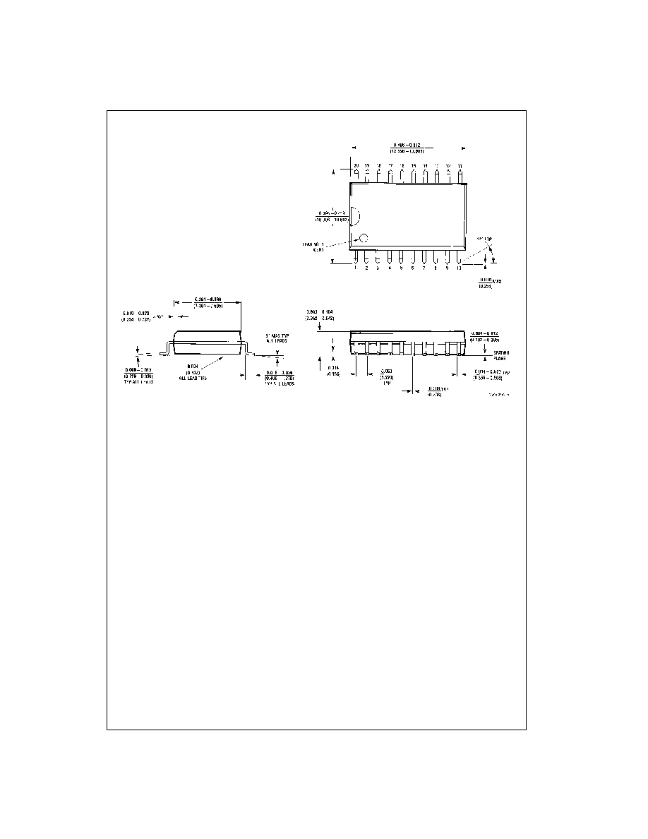
Physical Dimensions
inches (millimeters) unless otherwise noted
20-Lead Small Outline Integrated Circuit (SOIC), JEDEC MS-013, 0.300" Wide
Package Number M20B