September 1983
Revised February 1999
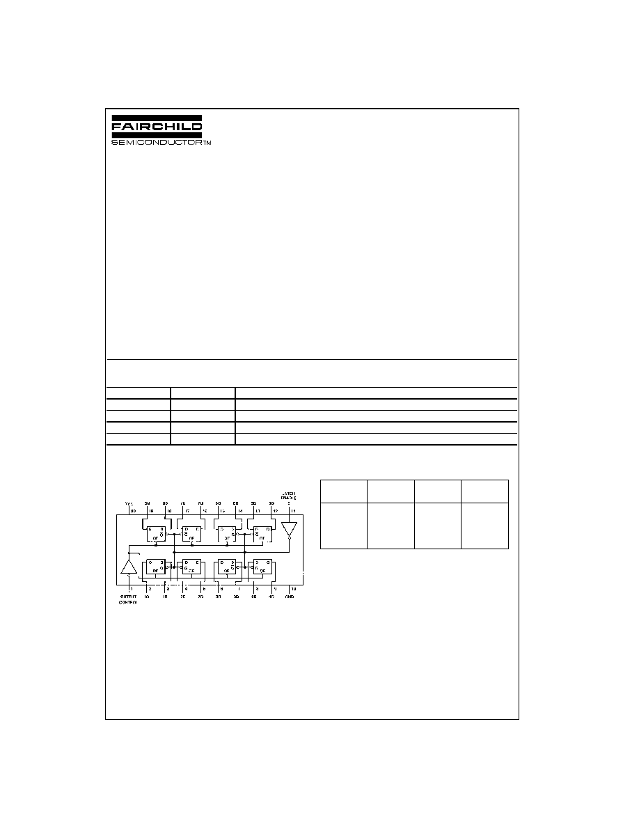
MM74HC373 3-ST
A
T
E
Oct
a
l D-T
ype Latc
h
© 1999 Fairchild Semiconductor Corporation
DS005335.prf
www.fairchildsemi.com
MM74HC373
3-STATE Octal D-Type Latch
General Description
The MM74HC373 high speed octal D-type latches utilize
advanced silicon-gate CMOS technology. They possess
the high noise immunity and low power consumption of
standard CMOS integrated circuits, as well as the ability to
drive 15 LS-TTL loads. Due to the large output drive capa-
bility and the 3-STATE feature, these devices are ideally
suited for interfacing with bus lines in a bus organized sys-
tem.
When the LATCH ENABLE input is HIGH, the Q outputs
will follow the D inputs. When the LATCH ENABLE goes
LOW, data at the D inputs will be retained at the outputs
until LATCH ENABLE returns HIGH again. When a high
logic level is applied to the OUTPUT CONTROL input, all
outputs go to a high impedance state, regardless of what
signals are present at the other inputs and the state of the
storage elements.
The 74HC logic family is speed, function, and pin-out com-
patible with the standard 74LS logic family. All inputs are
protected from damage due to static discharge by internal
diode clamps to V
CC
and ground.
Features
s
Typical propagation delay: 18 ns
s
Wide operating voltage range: 2 to 6 volts
s
Low input current: 1
µ
A maximum
s
Low quiescent current: 80
µ
A maximum (74 Series)
s
Output drive capability: 15 LS-TTL loads
Ordering Code:
Devices also available in Tape and Reel. Specify by appending the suffix letter "X" to the ordering code.
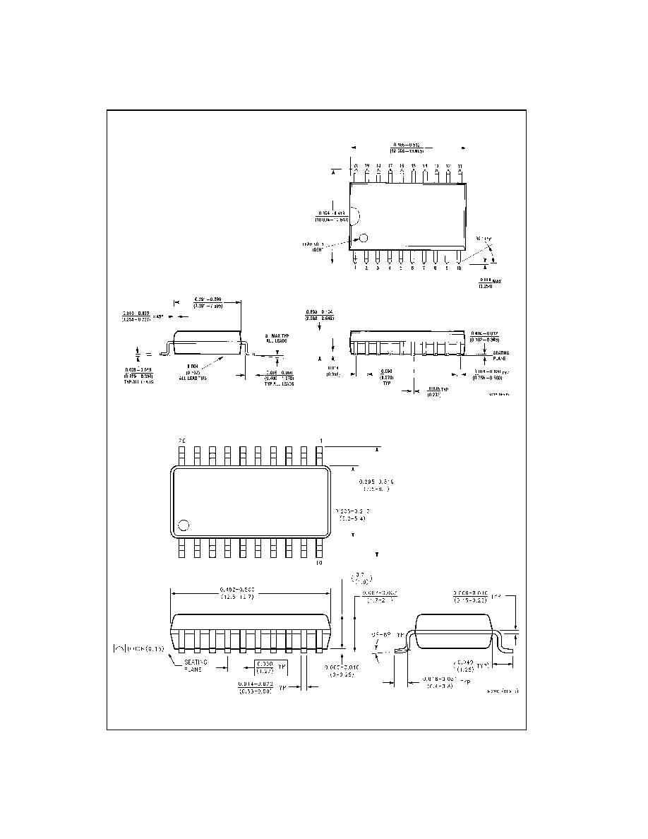
Connection Diagram
Pin Assignments for DIP, SOIC, SOP and TSSOP
Top View
Truth Table
H
=
HIGH Level
L
=
LOW Level
Q
0
=
Level of output before steady-state input conditions were established.
Z
=
High Impedance
Order Number
Package Number
Package Description
MM74HC373WM
M20B
20-Lead Small Outline Integrated Circuit (SOIC), JEDEC MS-013, 0.300" Wide
MM74HC373SJ
M20D
20-Lead Small Outline Package (SOP), EIAJ TYPE II, 5.3mm Wide
MM74HC373MTC
MTC20
20-Lead Thin Shrink Small Outline Package (TSSOP), JEDEC MO-153, 4.4mm Wide
MM74HC373N
N20A
20-Lead Plastic Dual-In-Line Package (PDIP), JEDEC MS-001, 0.300" Wide
Output
Latch
Data
373
Control
Enable
Output
L
H
H
H
L
H
L
L
L
L
X
Q
0
H
X
X
Z
www.fairchildsemi.com
2
MM
74HC373
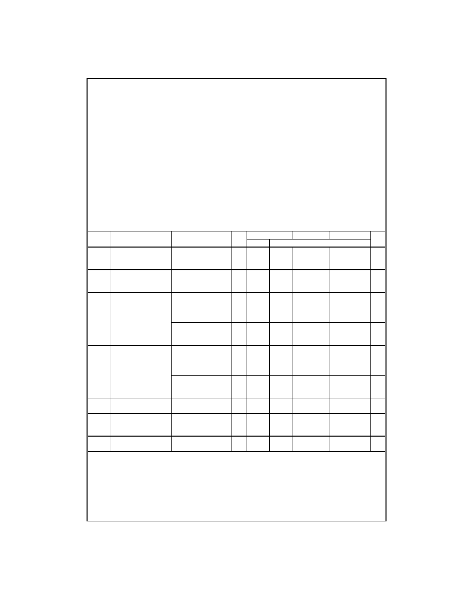
Absolute Maximum Ratings
(Note 1)
(Note 2)
Recommended Operating
Conditions
Note 1: Absolute Maximum Ratings are those values beyond which dam-
age to the device may occur.
Note 2: Unless otherwise specified all voltages are referenced to ground.
Note 3: Power Dissipation temperature derating -- plastic "N" package:
-
12 mW/
∞
C from 65
∞
C to 85
∞
C.
DC Electrical Characteristics
Note 4: For a power supply of 5V
±
10% the worst case output voltages (V
OH
, and V
OL
) occur for HC at 4.5V. Thus the 4.5V values should be used when
designing with this supply. Worst case V
IH
and V
IL
occur at V
CC
=
5.5V and 4.5V respectively. (The V
IH
value at 5.5V is 3.85V.) The worst case leakage cur-
rent (I
IN
, I
CC
, and I
OZ
) occur for CMOS at the higher voltage and so the 6.0V values should be used.
Supply Voltage (V
CC
)
-
0.5 to
+
7.0V
DC Input Voltage (V
IN
)
-
1.5 to V
CC
+
1.5V
DC Output Voltage (V
OUT
)
-
0.5 to V
CC
+
0.5V
Clamp Diode Current (I
IK
, I
OK
)
±
20 mA
DC Output Current, per pin (I
OUT
)
±
35 mA
DC V
CC
or GND Current, per pin (I
CC
)
±
70 mA
Storage Temperature Range (T
STG
)
-
65
∞
C to
+
150
∞
C
Power Dissipation (P
D
)
(Note 3)
600 mW
S.O. Package only
500 mW
Lead Temperature (T
L
)
(Soldering 10 seconds)
260
∞
C
Min
Max
Units
Supply Voltage (V
CC
)
2
6
V
DC Input or Output Voltage
(V
IN
,V
OUT
)
0
V
CC
V
Operating Temperature Range (T
A
)
-
40
+
85
∞
C
Input Rise or Fall Times
(t
r
, t
f
) V
CC
=
2.0V
1000
ns
V
CC
=
4.5V
500
ns
V
CC
=
6.0V
400
ns
Symbol
Parameter
Conditions
V
CC
T
A
=
25
∞
C
T
A
=
-
40 to 85
∞
C T
A
=
-
55 to 125
∞
C
Units
Typ
Guaranteed Limits
V
IH
Minimum HIGH Level
2.0V
1.5
1.5
1.5
V
Input Voltage
4.5V
3.15
3.15
3.15
V
6.0V
4.2
4.2
4.2
V
V
IL
Maximum LOW Level
2.0V
0.5
0.5
0.5
V
Input Voltage
4.5V
1.35
1.35
1.35
V
6.0V
1.8
1.8
1.8
V
V
OH
Minimum HIGH Level
V
IN
=
V
IH
or V
IL
Output Voltage
|I
OUT
|
20
µ
A
2.0V
2.0
1.9
1.9
1.9
V
4.5V
4.5
4.4
4.4
4.4
V
6.0V
6.0
5.9
5.9
5.9
V
V
IN
=
V
IH
or V
IL
|I
OUT
|
6.0 mA
4.5V
4.2
3.98
3.84
3.7
V
|I
OUT
|
7.8 mA
6.0V
5.7
5.48
5.34
5.2
V
V
OL
Maximum LOW Level
V
IN
=
V
IH
or V
IL
Output Voltage
|I
OUT
|
20
µ
A
2.0V
0
0.1
0.1
0.1
V
4.5V
0
0.1
0.1
0.1
V
6.0V
0
0.1
0.1
0.1
V
V
IN
=
V
IH
or V
IL
|I
OUT
|
6.0 mA
4.5V
0.2
0.26
0.33
0.4
V
|I
OUT
|
7.8 mA
6.0V
0.2
0.26
0.33
0.4
V
I
IN
Maximum Input
V
IN
=
V
CC
or GND
6.0V
±
0.1
±
1.0
±
1.0
µ
A
Current
I
OZ
Maximum 3-STATE
V
IN
=
V
IH
or V
IL
, OC
=
V
IH
6.0V
±
0.5
±
5
±
10
µ
A
Output Leakage
V
OUT
=
V
CC
or GND
Current
I
CC
Maximum Quiescent
V
IN
=
V
CC
or GND
6.0V
8.0
80
160
µ
A
Supply Current
I
OUT
=
0
µ
A
3
www.fairchildsemi.com
MM74HC373
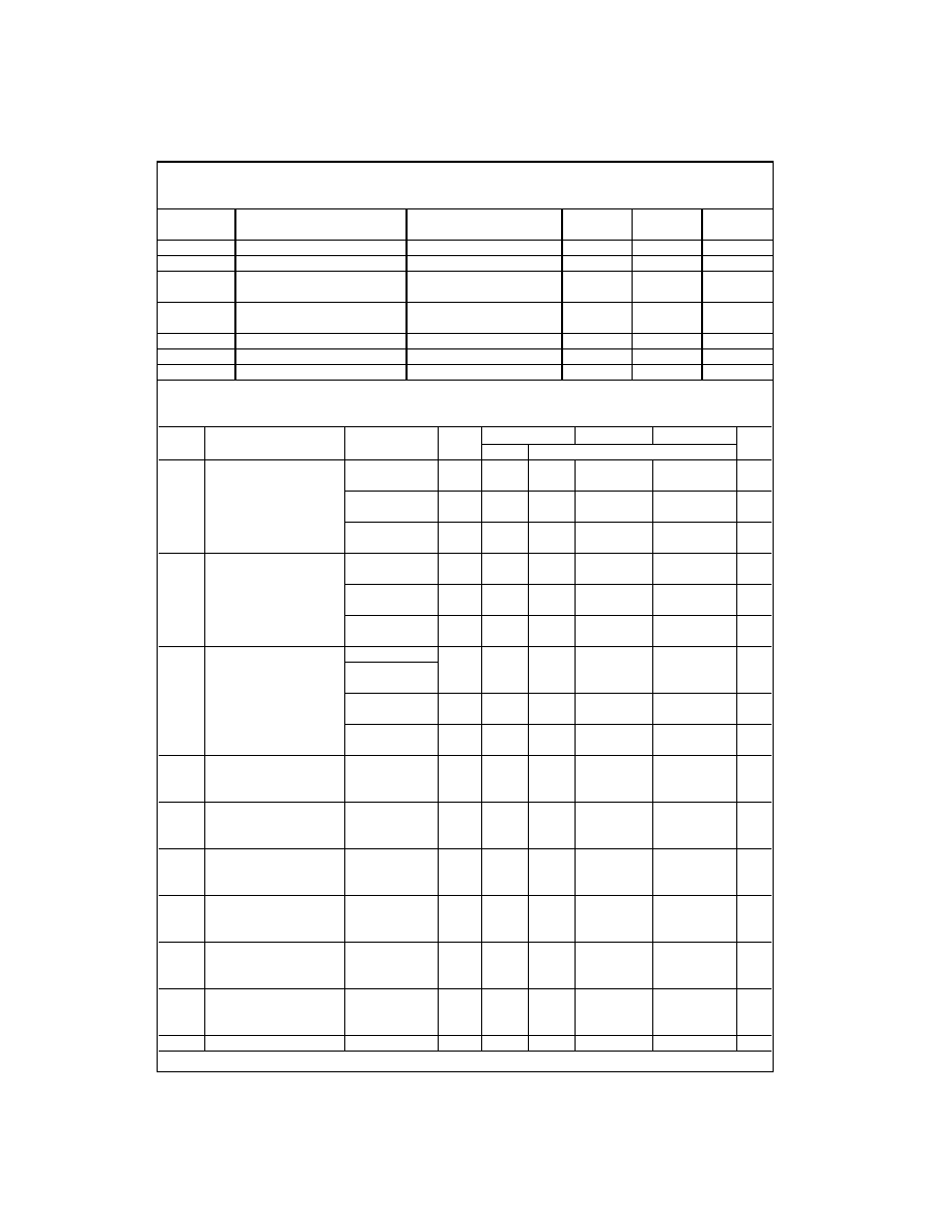
AC Electrical Characteristics
V
CC
=
5V, T
A
=
25
∞
C, t
r
=
t
f
=
6 ns
AC Electrical Characteristics
V
CC
=
2.0
-
6.0V, C
L
=
50 pF, t
r
=
t
f
=
6 ns (unless otherwise specified)
Symbol
Parameter
Conditions
Typ
Guaranteed
Units
Limit
t
PHL
, t
PLH
Maximum Propagation Delay, Data to Q C
L
=
45 pF
18
25
ns
t
PHL
, t
PLH
Maximum Propagation Delay, LE to Q
C
L
=
45 pF
21
30
ns
t
PZH
, t
PZL
Maximum Output Enable Time
R
L
=
1 k
20
28
ns
C
L
=
45 pF
t
PHZ
, t
PLZ
Maximum Output Disable Time
R
L
=
1 k
18
25
ns
C
L
=
5 pF
t
S
Minimum Set Up Time
5
ns
t
H
Minimum Hold Time
10
ns
t
W
Minimum Pulse Width
9
16
ns
Symbol
Parameter
Conditions
V
CC
T
A
=
25
∞
C
T
A
=
-
40 to 85
∞
C T
A
=
-
55 to 125
∞
C
Units
Typ
Guaranteed Limits
t
PHL
, t
PLH
Maximum Propagation
C
L
=
50 pF
2.0V
50
150
188
225
ns
Delay, Data to Q
C
L
=
150 pF
2.0V
80
200
250
300
ns
C
L
=
50 pF
4.5V
22
30
37
45
ns
C
L
=
150 pF
4.5V
30
40
50
60
ns
C
L
=
50 pF
6.0V
19
26
31
39
ns
C
L
=
150 pF
6.0V
26
35
44
53
ns
t
PHL
, t
PLH
Maximum Propagation
C
L
=
50 pF
2.0V
63
175
220
263
ns
Delay, LE to Q
C
L
=
150 pF
2.0V
110
225
280
338
ns
C
L
=
50 pF
4.5V
25
35
44
52
ns
C
L
=
150 pF
4.5V
35
45
56
68
ns
C
L
=
50 pF
6.0V
21
30
37
45
ns
C
L
=
150 pF
6.0V
28
39
49
59
ns
t
PZH
, t
PZL
Maximum Output
R
L
=
1 k
Enable Time
C
L
=
50 pF
2.0V
50
150
188
225
ns
C
L
=
150 pF
2.0V
80
200
250
300
ns
C
L
=
50 pF
4.5V
21
30
37
45
ns
C
L
=
150 pF
4.5V
30
40
50
60
ns
C
L
=
50 pF
6.0V
19
26
31
39
ns
C
L
=
150 pF
6.0V
26
35
44
53
ns
t
PHZ
, t
PLZ
Maximum Output Disable
R
L
=
1 k
2.0V
50
150
188
225
ns
Disable Time
C
L
=
50 pF
4.5V
21
30
37
45
ns
6.0V
19
26
31
39
ns
t
S
Minimum Set Up Time
2.0V
50
60
75
ns
4.5V
9
13
15
ns
6.0V
9
11
13
ns
t
H
Minimum Hold Time
2.0V
5
5
5
ns
4.5V
5
5
5
ns
6.0V
5
5
5
ns
t
W
Minimum Pulse Width
2.0V
30
80
100
120
ns
4.5V
10
16
20
24
ns
6.0V
9
14
18
20
ns
t
THL
, t
TLH
Maximum Output Rise
C
L
=
50 pF
2.0V
25
60
75
90
ns
and Fall Time
4.5V
7
12
15
18
ns
6.0V
6
10
13
15
ns
C
PD
Power Dissipation
(per latch)
Capacitance (Note 5)
OC
=
V
CC
30
pF
OC
=
GND
50
pF
C
IN
Maximum Input Capacitance
5
10
10
10
pF
www.fairchildsemi.com
4
MM
74HC373
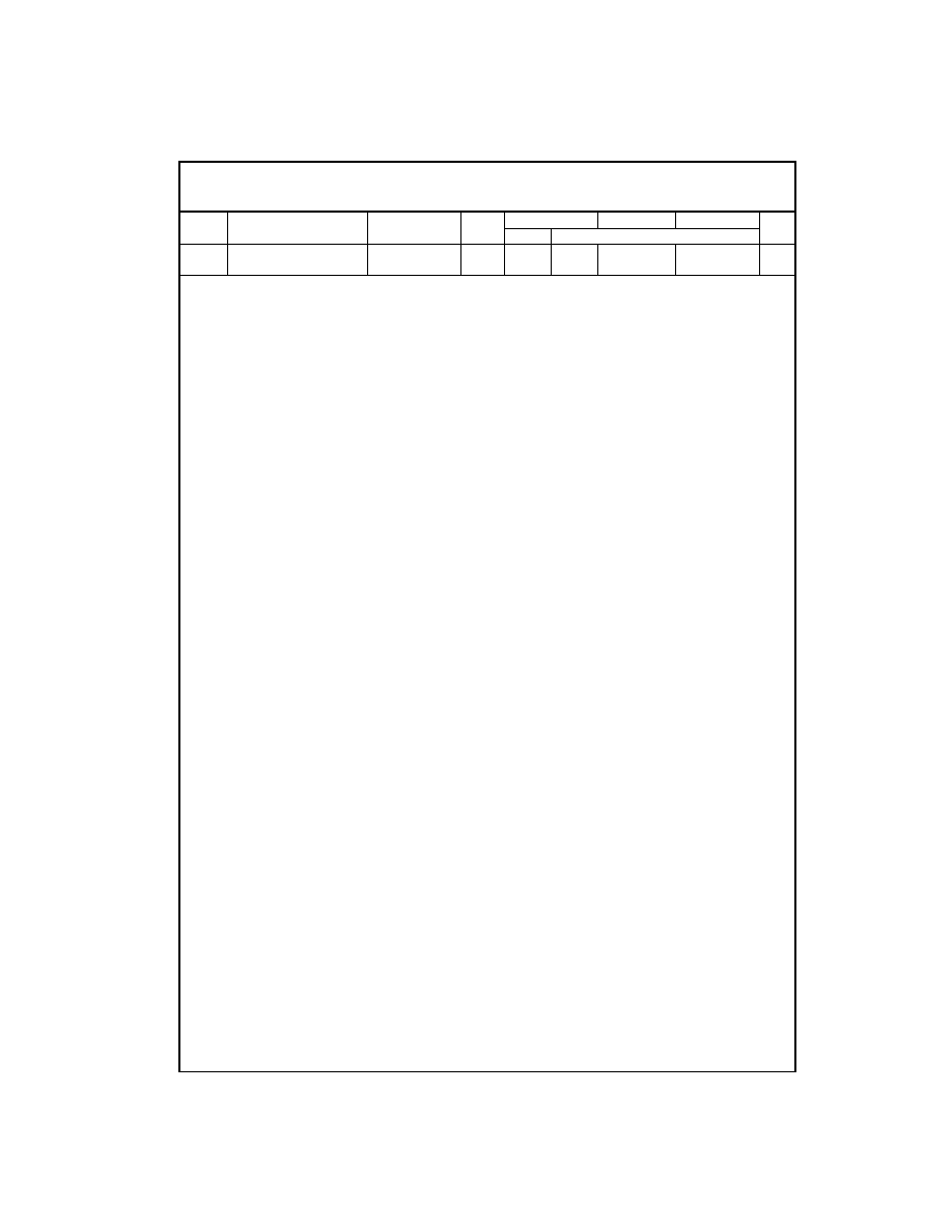
AC Electrical Characteristics
(Continued)
Note 5: C
PD
determines the no load dynamic power consumption, P
D
=
C
PD
V
CC
2
f
+
I
CC
V
CC
, and the no load dynamic current consumption,
I
S
=
C
PD
V
CC
f
+
I
CC
.
Symbol
Parameter
Conditions
V
CC
T
A
=
25
∞
C
T
A
=
-
40 to 85
∞
C T
A
=
-
55 to 125
∞
C
Units
Typ
Guaranteed Limits
C
OUT
Maximum Output
15
20
20
20
pF
Capacitance
5
www.fairchildsemi.com
MM74HC373
Physical Dimensions
inches (millimeters) unless otherwise noted
20-Lead Small Outline Integrated Circuit (SOIC), JEDEC MS-013, 0.300" Wide
Package Number M20B
20-Lead Small Outline Package (SOP), EIAJ TYPE II, 5.3mm Wide
Package Number M20D