February 1984
Revised February 1999
MM74HC4316
Quad Anal
og
Sw
i
t
ch
wit
h
L
evel
T
r
a
nslat
or
© 1999 Fairchild Semiconductor Corporation
DS005369.prf
www.fairchildsemi.com
MM74HC4316
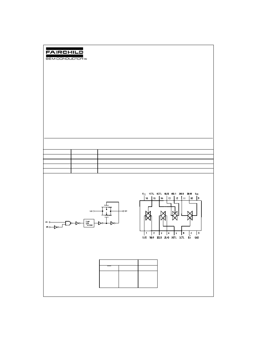
Quad Analog Switch with Level Translator
General Description
The MM74HC4316 devices are digitally controlled analog
switches implemented in advanced silicon-gate CMOS
technology. These switches have low "ON" resistance and
low "OFF" leakages. They are bidirectional switches, thus
any analog input may be used as an output and vice-versa.
Three supply pins are provided on the MM74HC4316 to
implement a level translator which enables this circuit to
operate with 0≠6V logic levels and up to
±
6V analog switch
levels. The MM74HC4316 also has a common enable input
in addition to each switch's control which when LOW will
disable all switches to their OFF state. All analog inputs
and outputs and digital inputs are protected from electro-
static damage by diodes to V
CC
and ground.
Features
s
Typical switch enable time: 20 ns
s
Wide analog input voltage range:
±
6V
s
Low "ON" resistance:
50 typ. (V
CC
-
V
EE
=
4.5V) 30 typ. (V
CC
-
V
EE
=
9V)
s
Low quiescent current: 80
µ
A maximum (74HC)
s
Matched switch characteristics
s
Individual switch controls plus a common enable
Ordering Code:
Devices also available in Tape and Reel. Specify by appending the suffix letter "X" to the ordering code.
Logic Diagram
Connection Diagram
Pin Assignments for DIP, SOIC, SOP and TSSOP
Top View
Truth Table
Order Number
Package Number
Package Description
MM74HC4316M
M16A
16-Lead Small Outline Integrated Package (SOIC), JEDEC MS-012, 0.150" Narrow
MM74HC4316SJ
M16D
16-Lead Small Outline Package (SOP), EIAJ TYPE II, 5.3mm Wide
MM74HC4316MTC
MTC16
16-Lead Thin Shrink Small Outline Package (TSSOP), JEDEC MO-1536, 4.4mm Wide
MM74HC4316N
N16E
16-Lead Plastic Dual-In-Line Package (PDIP), JEDEC MS-001, 0.300" Wide
Inputs
Switch
En
CTL
I/O≠O/I
H
X
"OFF"
L
L
"OFF"
L
H
"ON"
www.fairchildsemi.com
2
M
M
74HC4316
Absolute Maximum Ratings
(Note 1)
(Note 2)
Recommended Operating
Conditions
Note 1: Absolute Maximum Ratings are those values beyond which dam-
age to the device may occur.
Note 2: Unless otherwise specified all voltages are referenced to ground.
Note 3: Power Dissipation temperature derating -- plastic "N" package:
-
12 mW/
∞
C from 65
∞
C to 85
∞
C.
DC Electrical Characteristics
(Note 4)
Note 4: For a power supply of 5V
±
10% the worst case on resistances (R
ON
) occurs for HC at 4.5V. Thus the 4.5V values should be used when designing
with this supply. Worst case V
IH
and V
IL
occur at V
CC
=
5.5V and 4.5V respectively. (The V
IH
value at 5.5V is 3.85V.) The worst case leakage current occurs
for CMOS at the higher voltage and so the 5.5V values should be used.
Note 5: At supply voltages (V
CC
≠V
EE
) approaching 2V the analog switch on resistance becomes extremely non-linear. Therefore it is recommended that
these devices be used to transmit digital only when using these supply voltages.
Supply Voltage (V
CC
)
-
0.5 to
+
7.5V
Supply Voltage (V
EE
)
+
0.5 to
-
7.5V
DC Control Input Voltage (V
IN
)
-
1.5 to V
CC
+
1.5V
DC Switch I/O Voltage (V
IO
)
V
EE
-
0.5 to V
CC
+
0.5V
Clamp Diode Current (I
IK
, I
OK
)
±
20 mA
DC Output Current, per pin (I
OUT
)
±
25 mA
DC V
CC
or GND Current, per pin (I
CC
)
±
50 mA
Storage Temperature Range (T
STG
)
-
65
∞
C to
+
150
∞
C
Power Dissipation (P
D
)
(Note 3)
600 mW
S.O. Package only
500 mW
Lead Temperature (T
L
)
(Soldering 10 seconds)
260
∞
C
Min
Max
Units
Supply Voltage (V
CC
)
2
6
V
Supply Voltage (V
EE
)
0
-
6
V
DC Input or Output Voltage
(V
IN
, V
OUT
)
0
V
CC
V
Operating Temperature Range (T
A
)
-
40
+
85
∞
C
Input Rise or Fall Times
(t
r
, t
f
) V
CC
=
2.0V
1000
ns
V
CC
=
4.5V
500
ns
V
CC
=
6.0V
400
ns
V
CC
=
12.0V
250
ns
Symbol
Parameter
Conditions
V
EE
V
CC
T
A
=
25
∞
C
T
A
=
-
40 to 85
∞
C T
A
=
-
55 to 125
∞
C
Units
Typ
Guaranteed Limits
V
IH
Minimum HIGH Level
2.0V
1.5
1.5
1.5
V
Input Voltage
4.5V
3.15
3.15
3.15
V
6.0V
4.2
4.2
4.2
V
V
IL
Maximum LOW Level
2.0V
0.5
0.5
0.5
V
Input Voltage
4.5V
1.35
1.35
1.35
V
6.0V
1.8
1.8
1.8
V
R
ON
Minimum "ON" Resistance
V
CTL
=
V
IH
, I
S
=
2.0 mA
GND
4.5V
100
170
200
220
(Note 5)
V
IS
=
V
CC
to V
EE
-
4.5V
4.5V
40
85
105
110
(Figure 1)
-
6.0V
6.0V
30
70
85
90
GND
2.0V
100
180
215
240
V
CTL
=
V
IH
, I
S
=
2.0 mA
GND
4.5V
40
80
100
120
V
IS
=
V
CC
or V
EE
-
4.5V
4.5V
50
60
75
80
(Figure 1)
-
6.0V
6.0V
20
40
60
70
R
ON
Maximum "ON" Resistance
V
CTL
=
V
IH
GND
4.5V
10
15
20
20
Matching
V
IS
=
V
CC
to V
EE
-
4.5V
4.5V
5
10
15
15
-
6.0V
6.0V
5
10
15
15
I
IN
Maximum Control
V
IN
=
V
CC
or GND
GND
6.0V
±
0.1
±
1.0
±
1.0
µ
A
Input Current
I
IZ
Maximum Switch "OFF"
V
OS
=
V
CC
or V
EE
GND
6.0V
±
60
±
600
±
600
nA
Leakage Current
V
IS
=
V
EE
or V
CC
-
6.0V
6.0V
±
100
±
1000
±
1000
nA
V
CTL
=
V
IL
(Figure 2)
I
IZ
Maximum Switch "ON"
V
IS
=
V
CC
to V
EE
GND
6.0V
±
40
±
150
±
150
nA
Leakage Current
V
CTL
=
V
IH
, V
OS
=
OPEN
-
6.0V
6.0V
±
60
±
300
±
300
nA
(Figure 3)
I
CC
Maximum Quiescent
V
IN
=
V
CC
or GND
GND
6.0V
2.0
20
40
µ
A
Supply Current
I
OUT
=
0
µ
A
-
6.0V
6.0V
8.0
80
160
µ
A
3
www.fairchildsemi.com
MM74HC4316
AC Electrical Characteristics
V
CC
=
2.0V
-
6.0V, V
EE
=
0V
-
6V, C
L
=
50 pF (unless otherwise specified)
Note 6: Adjust 0 dBm for F
=
1 KHz (Null R
L
/Ron Attenuation).
Note 7: V
IS
is centered at V
CC
≠V
EE
/2.
Note 8: Adjust for 0 dBm.
Symbol
Parameter
Conditions
V
EE
V
CC
T
A
=
+
25
∞
C
T
A
=
-
40
∞
C to
+
85
∞
C T
A
=
-
55
∞
C to
+
125
∞
C
Units
Typ
Guaranteed Limits
t
PHL
, Maximum
Propagation
GND
2.0V
25
50
63
75
ns
t
PLH
Delay Switch
GND
4.5V
5
10
13
15
ns
In to Out
-
4.5V 4.5V
4
8
12
14
ns
-
6.0V 6.0V
3
7
11
13
ns
t
PZL
,
Maximum Switch
R
L
=
1 k
GND
2.0V
30
165
206
250
ns
t
PZH
Turn "ON" Delay
GND
4.5V
20
35
43
53
ns
(Control)
-
4.5V 4.5V
15
32
39
48
ns
-
6.0V 6.0V
14
30
37
45
ns
t
PHZ
,
Maximum Switch
R
L
=
1 k
GND
2.0V
45
250
312
375
ns
t
PLZ
Turn "OFF" Delay
GND
4.5V
25
50
63
75
ns
(Control)
-
4.5V 4.5V
20
44
55
66
ns
-
6.0V 6.0V
20
44
55
66
t
PZL
,
Maximum Switch
GND
2.0V
35
205
256
308
ns
t
PZH
Turn "ON" Delay
GND
4.5V
20
41
52
62
ns
(Enable)
-
4.5V 4.5V
19
38
48
57
ns
-
6.0V 6.0V
18
36
45
54
ns
t
PLZ
,
Maximum Switch
GND
2.0V
58
265
330
400
ns
t
PHZ
Turn "OFF" Delay
GND
4.5V
28
53
67
79
ns
(Enable)
-
4.5V 4.5V
23
47
59
70
ns
-
6.0V 6.0V
21
47
59
70
ns
f
MAX
Minimum Frequency
R
L
=
600
, V
IS
=
2V
PP
0V
4.5
40
MHz
Response (Figure 7)
at (V
CC
-
V
EE
/2)
-
4.5V 4.5V
100
MHz
20 log (V
OS
/V
IS
)
=
-
3 dB (Note 6) (Note 7)
Control to Switch
R
L
=
600
, F
=
1 MHz
0V
4.5V
100
mV
Feedthrough Noise
C
L
=
50 pF
-
4.5V 4.5V
250
mV
(Figure 8)
(Note 7) (Note 8)
Crosstalk Between
R
L
=
600
, F
=
1 MHz
any Two Switches
0V
4.5V
-
52
dB
(Figure 9)
-
4.5V 4.5V
-
50
dB
Switch OFF Signal
R
L
=
600
, F
=
1 MHz
Feedthrough Isolation
V
CTL
=
V
IL
,
0V
4.5V
-
42
dB
(Figure 10)
(Note 7) (Note 8)
-
4.5V 4.5V
-
44
dB
THD
Sinewave Harmonic
R
L
=
10 K
, C
L
=
50 pF,
Distortion
F
=
1 KHz
(Figure 11)
V
IS
=
4V
PP
0V
4.5V
0.013
%
V
IS
=
8V
PP
-
4.5V 4.5V
0.008
%
C
IN
Maximum Control
5
pF
Input Capacitance
C
IN
Maximum Switch
35
pF
Input Capacitance
C
IN
Maximum Feedthrough
V
CTL
=
GND
0.5
pF
Capacitance
C
PD
Power Dissipation
15
pF
Capacitance
www.fairchildsemi.com
4
M
M
74HC4316
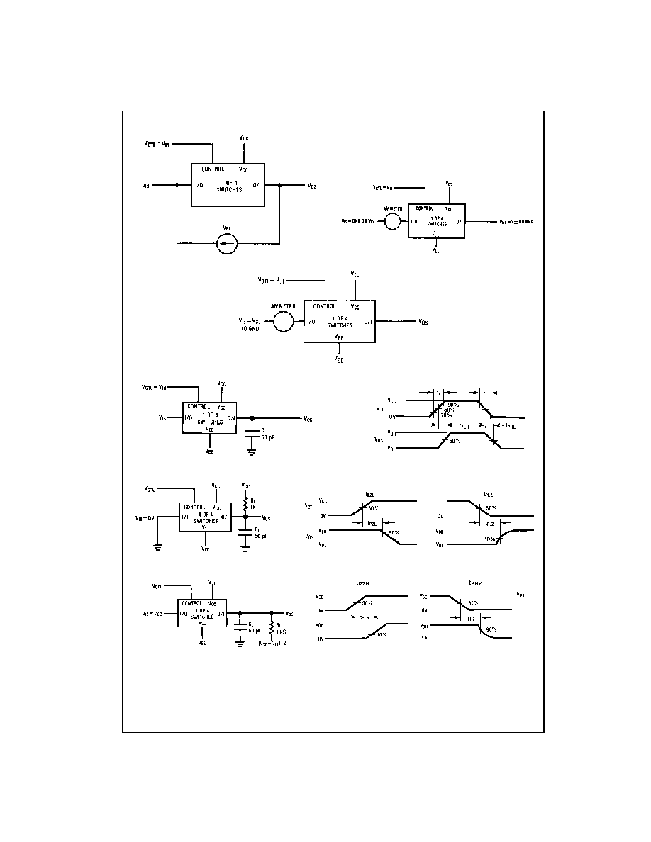
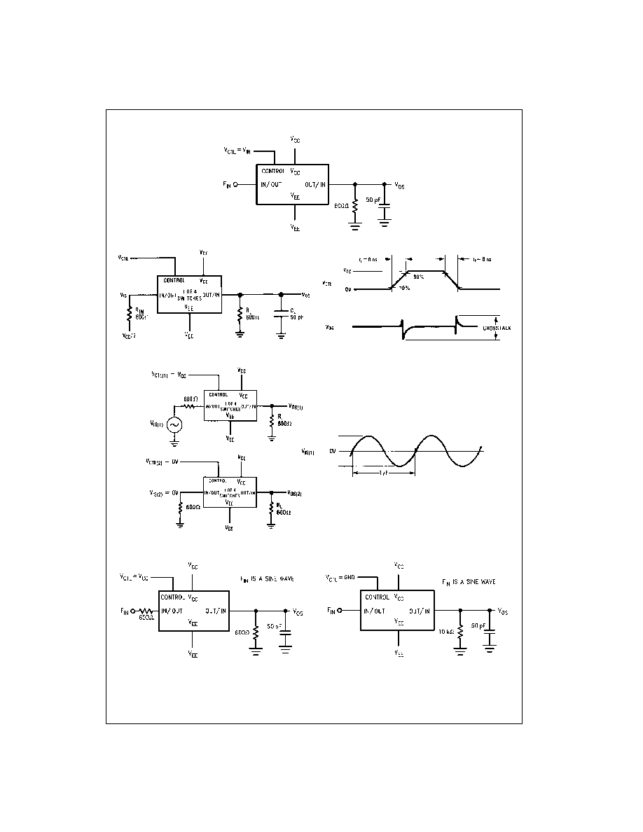
AC Test Circuits and Switching Time Waveforms
FIGURE 1. "ON" Resistance
FIGURE 2. "OFF" Channel Leakage Current
FIGURE 3. "ON" Channel Leakage Current
FIGURE 4. t
PHL
, t
PLH
Propagation Delay Time Signal Input to Signal Output
FIGURE 5. t
PZL
, t
PLZ
Propagation Delay Time Control to Signal Output
FIGURE 6. t
PZH
, t
PHZ
Propagation Delay Time Control to Signal Output
5
www.fairchildsemi.com
MM74HC4316
AC Test Circuits and Switching Time Waveforms
(Continued)
FIGURE 7. Frequency Response
FIGURE 8. Crosstalk: Control Input to Signal Output
FIGURE 9. : Crosstalk Between Any Two Switches
FIGURE 10. Switch OFF Signal Feedthrough Isolation
FIGURE 11. Sinewave Distortion