 | –≠–ª–µ–∫—Ç—Ä–æ–Ω–Ω—ã–π –∫–æ–º–ø–æ–Ω–µ–Ω—Ç: MM74HC573 | –°–∫–∞—á–∞—Ç—å:  PDF PDF  ZIP ZIP |
© 2000 Fairchild Semiconductor Corporation
DS005212
www.fairchildsemi.com
September 1983
Revised May 2000
MM74HC573 3-ST
A
T
E
Oct
a
l D-T
y
pe Lat
c
h
MM74HC573
3-STATE Octal D-Type Latch
General Description
The MM74HC573 high speed octal D-type latches utilize
advanced silicon-gate P-well CMOS technology. They pos-
sess the high noise immunity and low power consumption
of standard CMOS integrated circuits, as well as the ability
to drive 15 LS-TTL loads. Due to the large output drive
capability and the 3-STATE feature, these devices are ide-
ally suited for interfacing with bus lines in a bus organized
system.
When the LATCH ENABLE(LE) input is HIGH, the Q out-
puts will follow the D inputs. When the LATCH ENABLE
goes LOW, data at the D inputs will be retained at the out-
puts until LATCH ENABLE returns HIGH again. When a
HIGH logic level is applied to the OUTPUT CONTROL OC
input, all outputs go to a HIGH impedance state, regardless
of what signals are present at the other inputs and the state
of the storage elements.
The 74HC logic family is speed, function and pinout com-
patible with the standard 74LS logic family. All inputs are
protected from damage due to static discharge by internal
diode clamps to V
CC
and ground.
Features
s
Typical propagation delay: 18 ns
s
Wide operating voltage range: 2 to 6 volts
s
Low input current: 1
µ
A maximum
s
Low quiescent current: 80
µ
A maximum (74HC Series)
s
Compatible with bus-oriented systems
s
Output drive capability: 15 LS-TTL loads
Ordering Code:
Devices also available in Tape and Reel. Specify by appending the suffix letter "X" to the ordering code.
Connection Diagram
Top View
Truth Table
H
=
HIGH Level
L
=
LOW Level
Q
0
=
Level of output before steady-state input conditions were established.
Z
=
High Impedance
X
=
Don't Care
Order Number
Package Number
Package Description
MM74HC573WM
M20B
20-Lead Small Outline Integrated Circuit (SOIC), JEDEC MS-013, 0.300 Wide
MM74HC573SJ
M20D
20-Lead Small Outline Package (SOP), EIAJ TYPE II, 5.3mm Wide
MM74HC573MTC
MTC20
20-Lead Thin Shrink Small Outline Package (TSSOP), JEDEC MO-153, 4.4mm Wide
MM74HC573N
N20A
20-Lead Plastic Dual-In-Line Package (PDIP), JEDEC MS-001, 0.300 Wide
Output
Latch
Data
Output
Control
Enable
L
H
H
H
L
H
L
L
L
L
X
Q
0
H
X
X
Z
www.fairchildsemi.com
2
MM
74HC573
Absolute Maximum Ratings
(Note 1)
(Note 2)
Recommended Operating
Conditions
Note 1: Absolute Maximum Ratings are those values beyond which dam-
age to the device may occur.
Note 2: Unless otherwise specified all voltages are referenced to ground.
Note 3: Power Dissipation temperature derating -- plastic "N" package:
-
12 mW/
∞
C from 65
∞
C to 85
∞
C.
DC Electrical Characteristics
(Note 4)
Note 4: For a power supply of 5V
±
10% the worst-case output voltages (V
OH
, and V
OL
) occur for HC at 4.5V. Thus the 4.5V values should be used when
designing with this supply. Worst-case V
IH
and V
IL
occur at V
CC
=
5.5V and 4.5V respectively. (The V
IH
value at 5.5V is 3.85V.) The worst-case leakage cur-
rent (I
IN
, I
CC
, and I
OZ
) occur for CMOS at the higher voltage and so the 6.0V values should be used.
Supply Voltage (V
CC
)
-
0.5 to
+
7.0V
DC Input Voltage (V
IN
)
-
1.5 to V
CC
+
1.5V
DC Output Voltage (V
OUT
)
-
0.5 to V
CC
+
0.5V
Clamp Diode Current (I
IK
, I
OK
)
±
20 mA
DC Output Current, per pin (I
OUT
)
±
35 mA
DC V
CC
or GND Current, per pin (I
CC
)
±
70 mA
Storage Temperature Range (T
STG
)
-
65
∞
C to
+
150
∞
C
Power Dissipation (P
D
)
(Note 3)
600 mW
S.O. Package only
500 mW
Lead Temperature (T
L
)
(Soldering 10 seconds)
260
∞
C
Min
Max
Units
Supply Voltage (V
CC
)
2
6
V
DC Input or Output Voltage
0
V
CC
V
(V
IN
, V
OUT
)
Operating Temperature Range (T
A
)
-
40
+
85
∞
C
Input Rise or Fall Times
(t
r
, t
f
)
V
CC
=
2.0V
1000
ns
V
CC
=
4.5V
500
ns
V
CC
=
6.0V
400
ns
Symbol
Parameter
Conditions
V
CC
T
A
=
25
∞
C
T
A
=
-
40 to 85
∞
C T
A
=
-
55 to 125
∞
C
Units
Typ
Guaranteed Limits
V
IH
Minimum HIGH Level Input
2.0V
1.5
1.5
1.5
V
Voltage
4.5V
3.15
3.15
3.15
V
6.0V
4.2
4.2
4.2
V
V
IL
Maximum LOW Level Input
2.0V
0.5
0.5
0.5
V
Voltage 4.5V
1.35
1.35
1.35
V
6.0V
1.8
1.8
1.8
V
V
OH
Minimum HIGH Level Output
V
IN
=
V
IH
or V
IL
Voltage
|I
OUT
|
20
µ
A
2.0V
2.0
1.9
1.9
1.9
V
4.5V
4.5
4.4
4.4
4.4
V
6.0V
6.0
5.9
5.9
5.9
V
V
IN
=
V
IH
or V
IL
|I
OUT
|
6.0 mA
4.5V
4.2
3.98
3.84
3.7
V
|I
OUT
|
7.8 mA
6.0V
5.7
5.48
5.34
5.2
V
V
OL
Maximum LOW Level Output
V
IN
=
V
IH
or V
IL
Voltage
|I
OUT
|
20
µ
A
2.0V
0
0.1
0.1
0.1
V
4.5V
0
0.1
0.1
0.1
V
6.0V
0
0.1
0.1
0.1
V
V
IN
=
V
IH
or V
IL
|I
OUT
|
6.0 mA
4.5V
0.2
0.26
0.33
0.4
V
|I
OUT
|
7.8 mA
6.0V
0.2
0.26
0.33
0.4
V
I
IN
Maximum Input Current
V
IN
=
V
CC
or GND
6.0V
±
0.1
±
1.0
±
1.0
µ
A
I
OZ
Maximum 3-STATE Output
V
OUT
=
V
CC
or GND
Leakage Current
OC
=
V
IH
6.0V
±
0.5
±
5.0
±
10
µ
A
I
CC
Maximum Quiescent Supply
V
IN
=
V
CC
or GND
Current
I
OUT
=
0
µ
A
6.0V
8.0
80
160
µ
A
I
CC
Quiescent Supply Current
V
CC
=
5.5V
OE
1.0
1.5
1.8
2.0
mA
per Input Pin
V
IN
=
2.4V
LE
0.6
0.8
1.0
1.1
mA
or 0.4V (Note 4)
DATA
0.4
0.5
0.6
0.7
mA
3
www.fairchildsemi.com
MM74HC573
AC Electrical Characteristics
V
CC
=
5V, T
A
=
25
∞
C, t
r
=
t
f
=
6 ns
AC Electrical Characteristics
Symbol
Parameter
Conditions
Typ
Guaranteed
Units
Limit
t
PHL
, t
PLH
Maximum Propagation Delay, Data to Q
C
L
=
45 pF
16
20
ns
t
PHL
, t
PLH
Maximum Propagation Delay, LE to Q
C
L
=
45 pF
14
22
ns
t
PZH
, t
PZL
Maximum Output Enable Time
R
L
=
1 k
15
27
ns
C
L
=
45 pF
t
PHZ
, t
PLZ
Maximum Output Disable Time
R
L
=
1 k
13
23
ns
C
L
=
5 pF
t
S
Minimum Set Up Time, Data to LE
10
15
ns
t
H
Minimum Hold Time, LE to Data
2
5
ns
t
W
Minimum Pulse Width, LE or Data
10
16
ns
Symbol
Parameter
Conditions
V
CC
T
A
=
25
∞
C
T
A
=
-
40 to 85
∞
C T
A
=
-
55 to 125
∞
C
Units
Typ
Guaranteed Limits
t
PHL
, t
PLH
Maximum Propagation
C
L
=
50 pF
2.0V
45
110
138
165
ns
Delay Data to Q
C
L
=
150 pF
2.0V
58
150
188
225
ns
C
L
=
50 pF
4.5V
17
22
28
33
ns
C
L
=
150 pF
4.5V
21
30
38
40
ns
C
L
=
50 pF
6.0V
15
19
24
29
ns
C
L
=
150 pF
6.0V
19
26
33
39
ns
t
PHL
, t
PLH
Maximum Propagation
C
L
=
50 pF
2.0V
46
115
138
165
ns
Delay, LE to Q
C
L
=
150 pF
2.0V
60
155
194
233
ns
C
L
=
50 pF
4.5V
14
23
29
35
ns
C
L
=
150 pF
4.5V
21
31
47
47
ns
C
L
=
50 pF
6.0V
12
20
25
30
ns
C
L
=
150 pF
6.0V
19
27
34
41
ns
t
PZH
, t
PZL
Maximum Output Enable
R
L
=
1 k
Time
C
L
=
50 pF
2.0V
55
140
175
210
ns
C
L
=
150 pF
2.0V
67
180
225
270
ns
C
L
=
50 pF
4.5V
15
28
35
42
ns
C
L
=
150 pF
4.5V
24
36
45
54
ns
C
L
=
50 pF
6.0V
14
24
30
36
ns
C
L
=
150 pF
6.0V
22
31
39
47
ns
t
PHZ
, t
PLZ
Maximum Output Disable
R
L
=
1 k
2.0V
40
125
156
188
ns
Time
C
L
=
50 pF
4.5V
13
25
31
38
ns
6.0V
12
21
27
32
ns
t
S
Minimum Set Up Time
2.0V
30
75
95
110
ns
Data to LE
4.5V
10
15
19
22
ns
6.0V
9
13
16
19
ns
t
H
Minimum Hold Time
2.0V
25
31
38
ns
LE to Data
4.5V
5
6
7
ns
6.0V
4
5
6
ns
t
W
Minimum Pulse Width LE,
2.0V
30
80
100
120
ns
or Data
4.5V
9
16
20
24
ns
6.0V
8
14
18
20
ns
t
TLH
, t
THL
Maximum Output Rise
C
L
=
50 pF
2.0V
25
60
75
90
ns
and Fall Time, Clock
4.5V
7
12
15
18
ns
6.0V
6
10
13
15
ns
C
PD
Power Dissipation Capacitance
OC
=
V
CC
5
pF
(Note 5) (per latch)
OC
=
GND
52
pF
C
IN
Maximum Input
5
10
10
10
pF
Capacitance
www.fairchildsemi.com
4
MM
74HC573
AC Electrical Characteristics
(Continued)
Note 5: C
PD
determines the no load dynamic power consumption, P
D
=
C
PD
V
CC
2
f
+
I
CC
V
CC
, and the no load dynamic current consumption,
I
S
=
C
PD
V
CC
f
+
I
CC
.
Symbol
Parameter
Conditions
V
CC
T
A
=
25
∞
C
T
A
=
-
40 to 85
∞
C T
A
=
-
55 to 125
∞
C
Units
Typ
Guaranteed Limits
C
OUT
Maximum Output
15
20
20
20
pF
Capacitance
5
www.fairchildsemi.com
MM74HC573
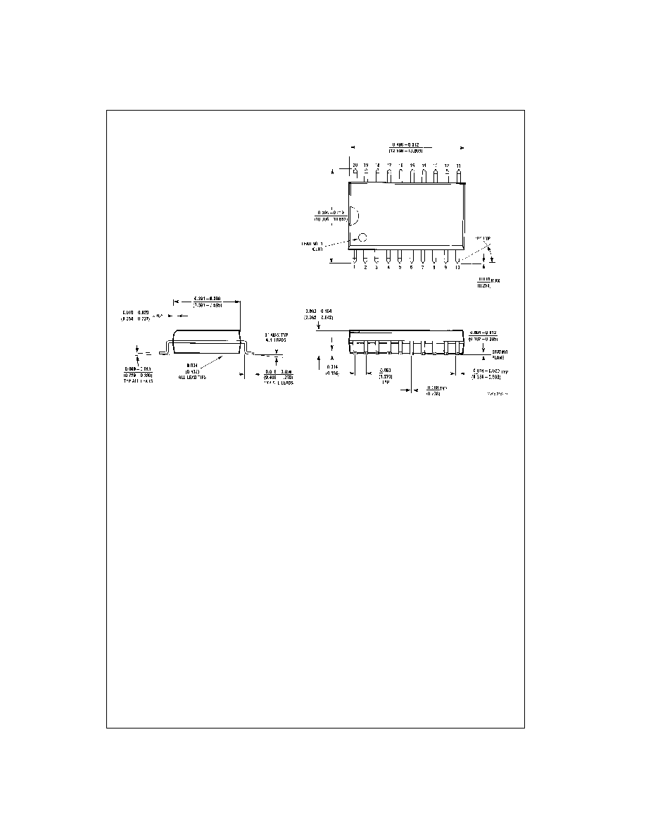
Physical Dimensions
inches (millimeters) unless otherwise noted
20-Lead Small Outline Integrated Circuit (SOIC), JEDEC MS-013, 0.300 Wide
Package Number M20B