September 1983
Revised February 1999
MM74HC595 8-Bi
t Shif
t Regi
ster
s
wi
th O
u
tput
Lat
ches
© 1999 Fairchild Semiconductor Corporation
DS005342.prf
www.fairchildsemi.com
MM74HC595
8-Bit Shift Registers with Output Latches
General Description
The MM74HC595 high speed shift register utilizes
advanced silicon-gate CMOS technology. This device pos-
sesses the high noise immunity and low power consump-
tion of standard CMOS integrated circuits, as well as the
ability to drive 15 LS-TTL loads.
This device contains an 8-bit serial-in, parallel-out shift reg-
ister that feeds an 8-bit D-type storage register. The stor-
age register has 8 3-STATE outputs. Separate clocks are
provided for both the shift register and the storage register.
The shift register has a direct-overriding clear, serial input,
and serial output (standard) pins for cascading. Both the
shift register and storage register use positive-edge trig-
gered clocks. If both clocks are connected together, the
shift register state will always be one clock pulse ahead of
the storage register.
The 74HC logic family is speed, function, and pin-out com-
patible with the standard 74LS logic family. All inputs are
protected from damage due to static discharge by internal
diode clamps to V
CC
and ground.
Features
s
Low quiescent current: 80
µ
A maximum (74HC Series)
s
Low input current: 1
µ
A maximum
s
8-bit serial-in, parallel-out shift register with storage
s
Wide operating voltage range: 2V≠6V
s
Cascadable
s
Shift register has direct clear
s
Guaranteed shift frequency: DC to 30 MHz
Ordering Code:
Devices also available in Tape and Reel. Specify by appending the suffix letter "X" to the ordering code.
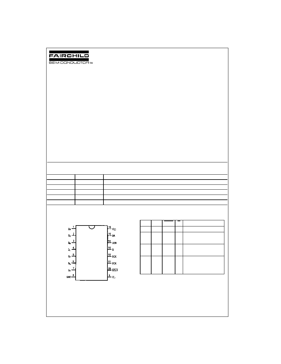
Connection Diagram
Pin Assignments for DIP, SOIC, SOP and TSSOP
Top View
Truth Table
Order Number
Package Number
Package Description
MM74HC595M
M16A
16-Lead Small Outline Integrated Circuit (SOIC), JEDEC MS-012, 0.150" Narrow
MM74HC595WM
M16B
16-Lead Small Outline Integrated Circuit (SOIC), JEDEC MS-013, 0.300" Wide
MM74HC595SJ
M16D
16-Lead Small Outline Package (SOP), EIAJ TYPE II, 5.3mm Wide
MM74HC595MTC
MTC16
16-Lead Thin Shrink Small Outline Package (TSSOP), JEDEC MO-153, 4.4mm Wide
MM74HC595N
N16E
16-Lead Dual-In-Line Package (PDIP), JEDEC MS-001, 0.300" Wide
RCK
SCK
SCLR
G
Function
X
X
X
H
Q
A
thru Q
H
=
3-STATE
X
X
L
L
Shift Register cleared
Q
H
=
0
X
H
L
Shift Register clocked
Q
N
=
Q
n-1
, Q
0
=
SER
X
H
L
Contents of Shift
Register transferred
to output latches
3
www.fairchildsemi.com
MM74HC595
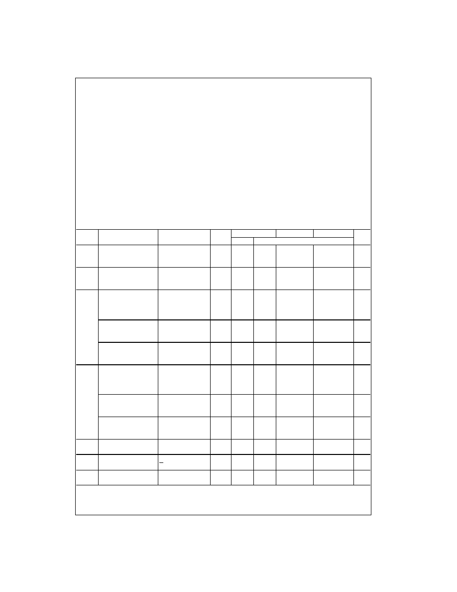
Absolute Maximum Ratings
(Note 1)
(Note 2)
Recommended Operating
Conditions
Note 1: Absolute Maximum Ratings are those values beyond which dam-
age to the device may occur.
Note 2: Unless otherwise specified all voltages are referenced to ground.
Note 3: Power Dissipation temperature derating -- plastic "N" package:
-
12 mW/
∞
C from 65
∞
C to 85
∞
C.
DC Electrical Characteristics
(Note 4)
Note 4: For a power supply of 5V
±
10% the worst case output voltages (V
OH
, and V
OL
) occur for HC at 4.5V. Thus the 4.5V values should be used when
designing with this supply. Worst case V
IH
and V
IL
occur at V
CC
=
5.5V and 4.5V respectively. (The V
IH
value at 5.5V is 3.85V.) The worst case leakage cur-
rent (I
IN
, I
CC
, and I
OZ
) occur for CMOS at the higher voltage and so the 6.0V values should be used.
Supply Voltage (V
CC
)
-
0.5 to
+
7.0V
DC Input Voltage (V
IN
)
-
1.5 to V
CC
+
1.5V
DC Output Voltage (V
OUT
)
-
0.5 to V
CC
+
0.5V
Clamp Diode Current (I
IK
, I
OK
)
±
20 mA
DC Output Current, per pin (I
OUT
)
±
35 mA
DC V
CC
or GND Current,
per pin (I
CC
)
±
70 mA
Storage Temperature Range (T
STG
)
-
65
∞
C to
+
150
∞
C
Power Dissipation (P
D
)
(Note 3)
600 mW
S.O. Package only
500 mW
Lead Temperature (T
L
)
(Soldering 10 seconds)
260
∞
C
Min
Max
Units
Supply Voltage (V
CC
)
2
6
V
DC Input or Output Voltage
(V
IN
, V
OUT
)
0
V
CC
V
Operating Temperature Range (T
A
)
-
40
+
85
∞
C
Input Rise or Fall Times
(t
r
, t
f
) V
CC
=
2.0V
1000
ns
V
CC
=
4.5V
500
ns
V
CC
=
6.0V
400
ns
Symbol
Parameter
Conditions
V
CC
T
A
=
25
∞
C
T
A
=
-
40 to 85
∞
C T
A
=
-
55 to 125
∞
C
Units
Typ
Guaranteed Limits
V
IH
Minimum HIGH Level
2.0V
1.5
1.5
1.5
V
Input Voltage
4.5V
3.15
3.15
3.15
V
6.0V
4.2
4.2
4.2
V
V
IL
Maximum LOW Level
2.0V
0.5
0.5
0.5
V
Input Voltage
4.5V
1.35
1.35
1.35
V
6.0V
1.8
1.8
1.8
V
V
OH
Minimum HIGH Level
V
IN
=
V
IH
or V
IL
Output Voltage
|I
OUT
|
20
µ
A
2.0V
2.0
1.9
1.9
1.9
V
4.5V
4.5
4.4
4.4
4.4
V
6.0V
6.0
5.9
5.9
5.9
V
Q
H
V
IN
=
V
IH
or V
IL
|I
OUT
|
4.0 mA
4.5V
4.2
3.98
3.84
3.7
V
|I
OUT
|
5.2 mA
6.0V
5.2
5.48
5.34
5.2
V
Q
A
thru Q
H
V
IN
=
V
IH
or V
IL
|I
OUT
|
6.0 mA
4.5V
4.2
3.98
3.84
3.7
V
|I
OUT
|
7.8 mA
6.0V
5.7
5.48
5.34
5.2
V
V
OL
Maximum LOW Level
V
IN
=
V
IH
or V
IL
Output Voltage
|I
OUT
|
20
µ
A
2.0V
0
0.1
0.1
0.1
V
4.5V
0
0.1
0.1
0.1
V
6.0V
0
0.1
0.1
0.1
V
Q
H
V
IN
=
V
IH
or V
IL
|I
OUT
|
4 mA
4.5V
0.2
0.26
0.33
0.4
V
|I
OUT
|
5.2 mA
6.0V
0.2
0.26
0.33
0.4
V
Q
A
thru Q
H
V
IN
=
V
IH
or V
IL
|I
OUT
|
6.0 mA
4.5V
0.2
0.26
0.33
0.4
V
|I
OUT
|
7.8 mA
6.0V
0.2
0.26
0.33
0.4
V
I
IN
Maximum Input
V
IN
=
V
CC
or GND
6.0V
±
0.1
±
1.0
±
1.0
µ
A
Current
I
OZ
Maximum 3-STATE
V
OUT
=
V
CC
or GND
6.0V
±
0.5
±
5.0
±
10
µ
A
Output Leakage
G
=
V
IH
I
CC
Maximum Quiescent
V
IN
=
V
CC
or GND
6.0V
8.0
80
160
µ
A
Supply Current
I
OUT
=
0
µ
A
www.fairchildsemi.com
4
MM
74HC595
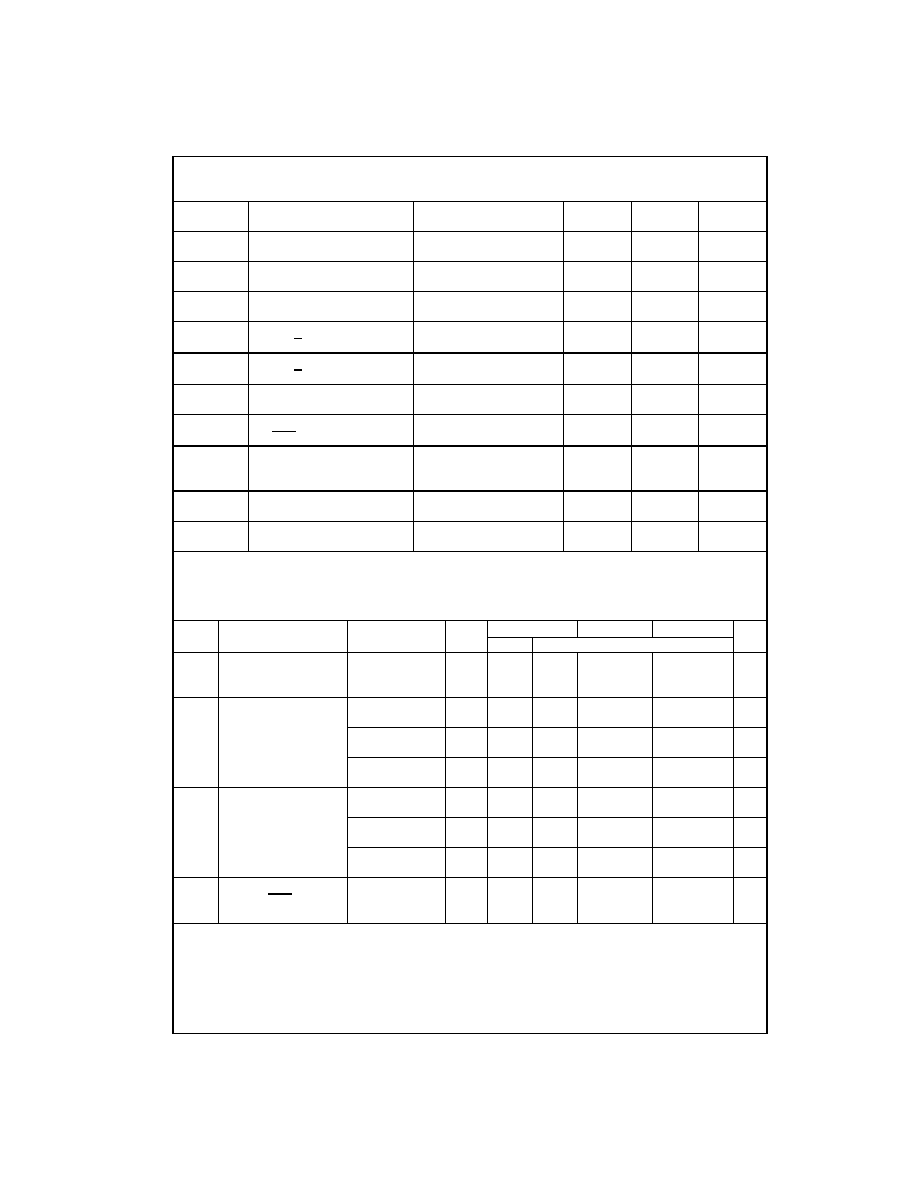
AC Electrical Characteristics
V
CC
=
5V, T
A
=
25
∞
C, t
r
=
t
f
=
6 ns
Note 5: This setup time ensures the register will see stable data from the shift-register outputs. The clocks may be connected together in which case the stor-
age register state will be one clock pulse behind the shift register.
AC Electrical Characteristics
V
CC
=
2.0
-
6.0V, C
L
=
50 pF, t
r
=
t
f
=
6 ns (unless otherwise specified)
Symbol
Parameter
Conditions
Typ
Guaranteed
Units
Limit
f
MAX
Maximum Operating
50
30
MHz
Frequency of SCK
t
PHL
, t
PLH
Maximum Propagation
C
L
=
45 pF
12
20
ns
Delay, SCK to Q
H'
t
PHL
, t
PLH
Maximum Propagation
C
L
=
45 pF
18
30
ns
Delay, RCK to Q
A
thru Q
H
t
PZH
, t
PZL
Maximum Output Enable
R
L
=
1 k
Time from G to Q
A
thru Q
H
C
L
=
45 pF
17
28
ns
t
PHZ
, t
PLZ
Maximum Output Disable
R
L
=
k
15
25
ns
Time from G to Q
A
thru Q
H
C
L
=
5 pF
t
S
Minimum Setup Time
20
ns
from SER to SCK
t
S
Minimum Setup Time
20
ns
from SCLR to SCK
t
S
Minimum Setup Time
40
ns
from SCK to RCK
(Note 5)
t
H
Minimum Hold Time
0
ns
from SER to SCK
t
W
Minimum Pulse Width
16
ns
of SCK or RCK
Symbol
Parameter
Conditions
V
CC
T
A
=
25
∞
C
T
A
=
-
40 to 85
∞
C T
A
=
-
55 to 125
∞
C
Units
Typ
Guaranteed Limits
f
MAX
Maximum Operating
C
L
=
50 pF
2.0V
10
6
4.8
4.0
MHz
Frequency
4.5V
45
30
24
20
MHz
6.0V
50
35
28
24
MHz
t
PHL
, t
PLH
Maximum Propagation
C
L
=
50 pF
2.0V
58
210
265
315
ns
Delay from SCK to Q
H
C
L
=
150 pF
2.0V
83
294
367
441
ns
C
L
=
50 pF
4.5V
14
42
53
63
ns
C
L
=
150 pF
4.5V
17
58
74
88
ns
C
L
=
50 pF
6.0V
10
36
45
54
ns
C
L
=
150 pF
6.0V
14
50
63
76
ns
t
PHL
, t
PLH
Maximum Propagation
C
L
=
50 pF
2.0V
70
175
220
265
ns
Delay from RCK to Q
A
thru Q
H
C
L
=
150 pF
2.0V
105
245
306
368
ns
C
L
=
50 pF
4.5V
21
35
44
53
ns
C
L
=
150 pF
4.5V
28
49
61
74
ns
C
L
=
50 pF
6.0V
18
30
37
45
ns
C
L
=
150 pF
6.0V
26
42
53
63
ns
t
PHL
, t
PLH
Maximum Propagation
2.0V
175
221
261
ns
Delay from SCLR to Q
H
4.5V
35
44
52
ns
6.0V
30
37
44
ns
5
www.fairchildsemi.com
MM74HC595
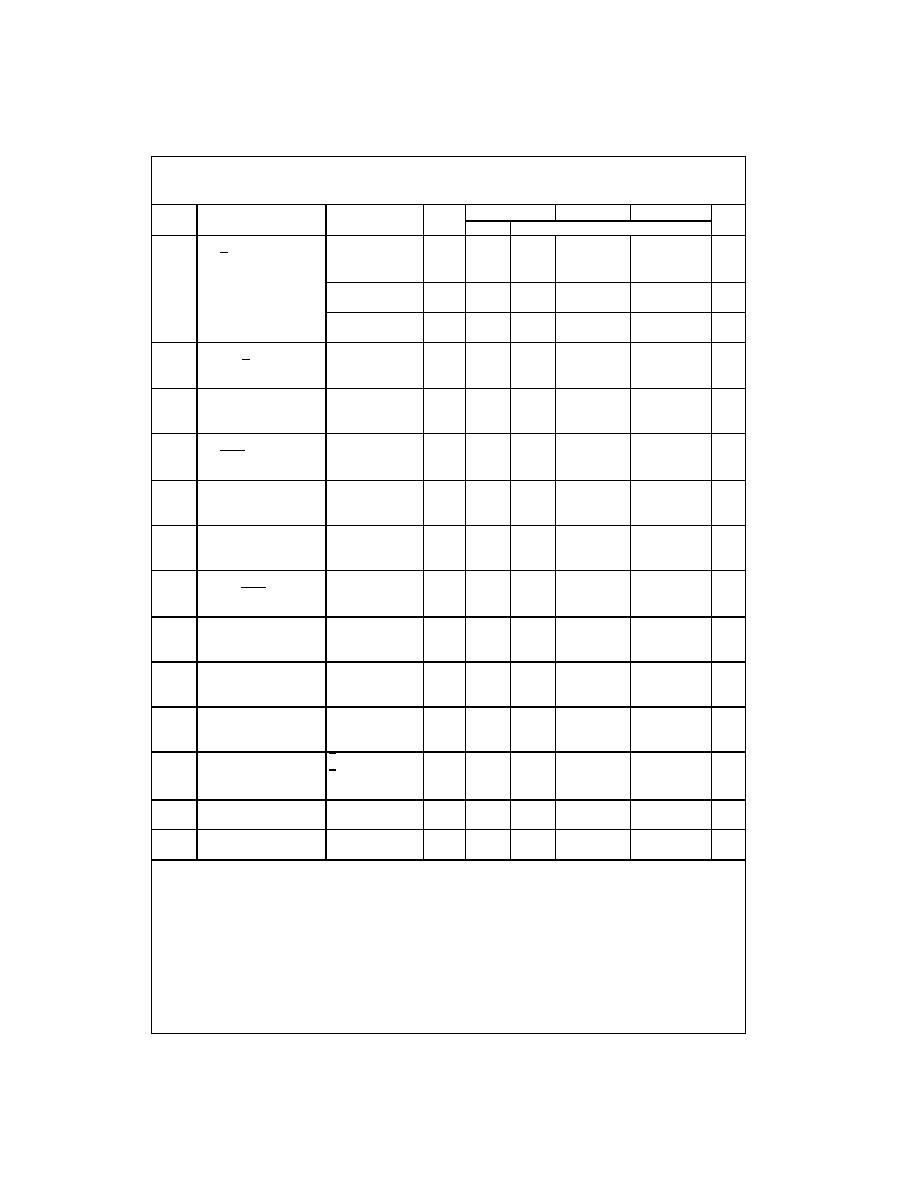
AC Electrical Characteristics
(Continued)
Note 6: C
PD
determines the no load dynamic power consumption, P
D
=
C
PD
V
CC
2
f
+
I
CC
V
CC
, and the no load dynamic current consumption,
I
S
=
C
PD
V
CC
f
+
I
CC
.
Symbol
Parameter
Conditions
V
CC
T
A
=
25
∞
C
T
A
=
-
40 to 85
∞
C T
A
=
-
55 to 125
∞
C
Units
Typ
Guaranteed Limits
t
PZH
, t
PZL
Maximum Output Enable
R
L
=
1 k
from G to Q
A
thru Q
H
C
L
=
50 pF
2.0V
75
175
220
265
ns
C
L
=
150 pF
2.0V
100
245
306
368
ns
C
L
=
50 pF
4.5V
15
35
44
53
ns
C
L
=
150 pF
4.5V
20
49
61
74
ns
C
L
=
50 pF
6.0V
13
30
37
45
ns
C
L
=
150 pF
6.0V
17
42
53
63
ns
t
PHZ
, t
PLZ
Maximum Output Disable
R
L
=
1 k
2.0V
75
175
220
265
ns
Time from G to Q
A
thru Q
H
C
L
=
50 pF
4.5V
15
35
44
53
ns
6.0V
13
30
37
45
ns
t
S
Minimum Setup Time
2.0V
100
125
150
ns
from SER to SCK
4.5V
20
25
30
ns
6.0V
17
21
25
ns
t
R
Minimum Removal Time
2.0V
50
63
75
ns
from SCLR to SCK
4.5V
10
13
15
ns
6.0V
9
11
13
ns
t
S
Minimum Setup Time
2.0V
100
125
150
ns
from SCK to RCK
4.5V
20
25
30
ns
6.0V
17
21
26
ns
t
H
Minimum Hold Time
2.0V
5
5
5
ns
SER to SCK
4.5V
5
5
5
ns
6.0V
5
5
5
ns
t
W
Minimum Pulse Width
2.0V
30
80
100
120
ns
of SCK or SCLR
4.5V
9
16
20
24
ns
6.0V
8
14
18
22
ns
t
r
, t
f
Maximum Input Rise and
2.0V
1000
1000
1000
ns
Fall Time, Clock
4.5V
500
500
500
ns
6.0V
400
400
400
ns
t
THL
, t
TLH
Maximum Output
2.0V
25
60
75
90
ns
Rise and Fall Time
4.5V
7
12
15
18
ns
Q
A
≠Q
H
6.0V
6
10
13
15
ns
t
THL
, t
TLH
Maximum Output
2.0V
75
95
110
ns
Rise & Fall Time
4.5V
15
19
22
ns
Q
H
6.0V
13
16
19
ns
C
PD
Power Dissipation
G
=
V
CC
90
pF
Capacitance, Outputs
G
=
GND
150
pF
Enabled (Note 6)
C
IN
Maximum Input
5
10
10
10
pF
Capacitance
C
OUT
Maximum Output
15
20
20
20
pF
Capacitance
