
September 1983
Revised February 1999
MM74HC688 8-Bi
t Magnit
ude C
o
m
par
ator
(
E
quali
t
y
Det
ector
)
© 1999 Fairchild Semiconductor Corporation
DS005018.prf
www.fairchildsemi.com
MM74HC688
8-Bit Magnitude Comparator (Equality Detector)
General Description
The MM74HC688 equality detector utilizes advanced sili-
con-gate CMOS technology to compare bit for bit two 8-bit
words and indicates whether or not they are equal. The
P
=
Q output indicates equality when it is LOW. A single
active low enable is provided to facilitate cascading of sev-
eral packages and enable comparison of words greater
than 8 bits.
This device is useful in memory block decoding applica-
tions, where memory block enable signals must be gener-
ated from computer address information.
The comparator's output can drive 10 low power Schottky
equivalent loads. This comparator is functionally and pin
compatible to the 74LS688. All inputs are protected from
damage due to static discharge by diodes to V
CC
and
ground.
Features
s
Typical propagation delay: 20 ns
s
Wide power supply range: 2≠6V
s
Low quiescent current: 80
µ
A (74 Series)
s
Large output current: 4 mA (74 Series)
s
Same as HC521
Ordering Code:
Devices also available in Tape and Reel. Specify by appending the suffix letter "X" to the ordering code.
Connection Diagram
Pin Assignments for DIP
Top View
Truth Table
Logic Diagram
Order Number
Package Number
Package Description
MM74HC688WM
M20B
20-Lead Small Outline Integrated Circuit (SOIC), JEDEC MS-013, 0.300" Wide
MM74HC688SJ
M20D
20-Lead Small Outline Package (SOP), EIAJ TYPE II, 5.3mm Wide
MM74HC688MTC
MTC20
20-Lead Thin Shrink Small Outline Package (TSSOP), JEDEC MO-153, 4.4mm Wide
MM74HC688N
N20A
20-Lead Plastic Dual-In-Line Package (PDIP), JEDEC MS-001, 0.300" Wide
Inputs
Data
Enable
P,Q
G
P
=
Q
P
=
Q
L
L
P
>
Q
L
H
P
<
Q
L
H
X
H
H

www.fairchildsemi.com
2
MM
74HC688
Absolute Maximum Ratings
(Note 1)
(Note 2)
Recommended Operating
Conditions
Note 1: Absolute Maximum Ratings are those values beyond which dam-
age to the device may occur.
Note 2: Unless otherwise specified all voltages are referenced to ground.
Note 3: Power Dissipation temperature derating -- plastic "N" package:
-
12 mW/
∞
C from 65
∞
C to 85
∞
C.
DC Electrical Characteristics
(Note 4)
Note 4: For a power supply of 5V
±
10% the worst case output voltages (V
OH
, and V
OL
) occur for HC at 4.5V. Thus the 4.5V values should be used when
designing with this supply. Worst case V
IH
and V
IL
occur at V
CC
=
5.5V and 4.5V respectively. (The V
IH
value at 5.5V is 3.85V.) The worst case leakage cur-
rent (I
IN
, I
CC
, and I
OZ
) occur for CMOS at the higher voltage and so the 6.0V values should be used.
Supply Voltage (V
CC
)
-
0.5 to
+
7.0V
DC Input Voltage (V
IN
)
-
1.5 to V
CC
+
1.5V
DC Output Voltage (V
OUT
)
-
0.5 to V
CC
+
0.5V
Clamp Diode Current (I
IK
, I
OK
)
±
20 mA
DC Output Current, per pin (I
OUT
)
±
25 mA
DC V
CC
or GND Current, per pin
(I
CC
)
±
50 mA
Storage Temperature Range (T
STG
)
-
65
∞
C to
+
150
∞
C
Power Dissipation (P
D
)
(Note 3)
600 mW
S.O. Package only
500 mW
Lead Temperature (T
L
)
(Soldering 10 seconds)
260
∞
C
Min
Max
Units
Supply Voltage (V
CC
)
2
6
V
DC Input or Output Voltage
0
V
CC
V
(V
IN
, V
OUT
)
Operating Temperature Range (T
A
)
-
40
+
85
∞
C
Input Rise or Fall Times
(t
r
, t
f
) V
CC
=
2.0V
1000
ns
V
CC
=
4.5V
500
ns
V
CC
=
6.0V
400
ns
Symbol
Parameter
Conditions
V
CC
T
A
=
25
∞
C
T
A
=
-
40 to 85
∞
C T
A
=
-
55 to 125
∞
C
Units
Typ
Guaranteed Limits
V
IH
Minimum HIGH Level
2.0V
1.5
1.5
1.5
V
Input Voltage
4.5V
3.15
3.15
3.15
V
6.0V
4.2
4.2
4.2
V
V
IL
Maximum LOW Level
2.0V
0.5
0.5
0.5
V
Input Voltage
4.5V
1.35
1.35
1.35
V
6.0V
1.8
1.8
1.8
V
V
OH
Minimum HIGH Level
V
IN
=
V
IH
or V
IL
Output Voltage
|I
OUT
|
20
µ
A
2.0V
2.0
1.9
1.9
1.9
V
4.5V
4.5
4.4
4.4
4.4
V
6.0V
6.0
5.9
5.9
5.9
V
V
IN
=
V
IH
or V
IL
|I
OUT
|
4.0 mA
4.5V
4.2
3.98
3.84
3.7
V
|I
OUT
|
5.2 mA
6.0V
5.7
5.48
5.34
5.2
V
V
OL
Maximum LOW Level
V
IN
=
V
IH
or V
IL
Output Voltage
|I
OUT
|
20
µ
A
2.0V
0
0.1
0.1
0.1
V
4.5V
0
0.1
0.1
0.1
V
6.0V
0
0.1
0.1
0.1
V
V
IN
=
V
IH
or V
IL
|I
OUT
|
4.0 mA
4.5V
0.2
0.26
0.33
0.4
V
|I
OUT
|
5.2 mA
6.0V
0.2
0.26
0.33
0.4
V
I
IN
Maximum Input
V
IN
=
V
CC
or GND
6.0V
±
0.1
±
1.0
±
1.0
µ
A
Current
I
CC
Maximum Quiescent
V
IN
=
V
CC
or GND
6.0V
8.0
80
160
µ
A
Supply Current
I
OUT
=
0
µ
A

3
www.fairchildsemi.com
MM74HC688
AC Electrical Characteristics
V
CC
=
5V, T
A
=
25
∞
C, C
L
=
15 pF, t
r
=
t
f
=
6 ns
AC Electrical Characteristics
V
CC
=
2.0V to 6.0V, C
L
=
50 pF, t
r
=
t
f
=
6 ns (unless otherwise specified)
Note 5: C
PD
determines the no load dynamic power consumption, P
D
=
C
PD
V
CC
2
f
+
I
CC
V
CC
, and the no load dynamic current consumption,
I
S
=
C
PD
V
CC
f
+
I
CC
.
Symbol
Parameter
Conditions
Typ
Guaranteed
Units
Limit
t
PHL
, t
PLH
Maximum Propagation
21
30
ns
Delay, any P or Q to Output
t
PLH
, t
PHL
Maximum Propagation
14
20
ns
Delay, Enable to any Output
Symbol
Parameter
Conditions
V
CC
T
A
=
25
∞
C
T
A
=
-
40 to 85
∞
C T
A
=
-
55 to 125
∞
C
Units
Typ
Guaranteed Limits
t
PHL
, t
PLH
Maximum Propagation
2.0V
60
175
220
263
ns
Delay, P or Q to
4.5V
22
35
44
53
ns
Output
6.0V
19
30
38
45
ns
t
PHL
, t
PLH
Maximum Propagation
2.0V
45
120
150
180
ns
Delay, Enable to
4.5V
15
24
30
36
ns
Output
6.0V
13
20
25
30
ns
t
THL
, t
TLH
Maximum Output Rise
2.0V
30
75
95
110
ns
and Fall Time
4.5V
8
15
19
22
ns
6.0V
7
13
16
19
ns
C
PD
Power Dissipation
45
pF
Capacitance (Note 5)
C
IN
Maximum Input
5
10
10
10
pF
Capacitance
www.fairchildsemi.com
4
MM
74HC688
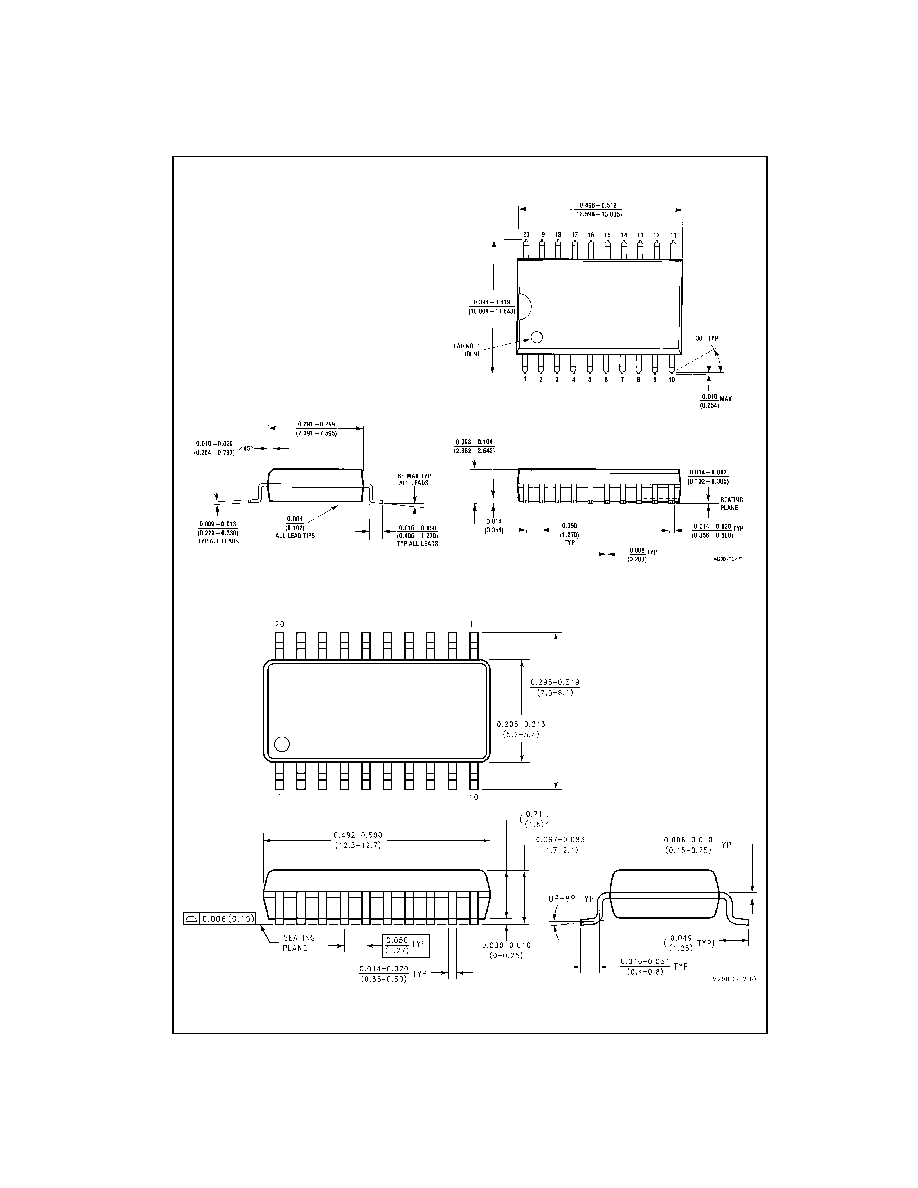
Physical Dimensions
inches (millimeters) unless otherwise noted
20-Lead Small Outline Integrated Circuit (SOIC), JEDEC MS-013, 0.300" Wide
Package Number M20B
20-Lead Small Outline Package (SOP), EIAJ TYPE II, 5.3mm Wide
Package Number M20D
5
www.fairchildsemi.com
MM74HC688
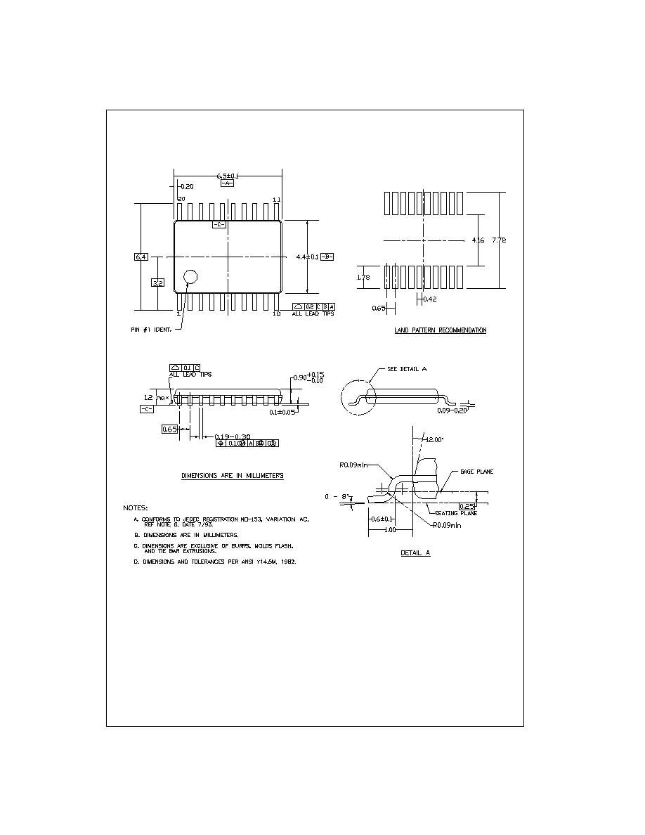
Physical Dimensions
inches (millimeters) unless otherwise noted (Continued)
20-Lead Thin Shrink Small Outline Package (TSSOP), JEDEC MO-153, 4.4mm Wide
Package Number MTC20