© 2005 Fairchild Semiconductor Corporation
DS005106
www.fairchildsemi.com
September 1983
Revised January 2005
MM74HC74A D
u
a
l
D-T
y
pe Fli
p
-Fl
op w
i
t
h
Pre
set and C
l
ear
MM74HC74A
Dual D-Type Flip-Flop with Preset and Clear
General Description
The MM74HC74A utilizes advanced silicon-gate CMOS
technology to achieve operating speeds similar to the
equivalent LS-TTL part. It possesses the high noise immu-
nity and low power consumption of standard CMOS inte-
grated circuits, along with the ability to drive 10 LS-TTL
loads.
This flip-flop has independent data, preset, clear, and clock
inputs and Q and Q outputs. The logic level present at the
data input is transferred to the output during the positive-
going transition of the clock pulse. Preset and clear are
independent of the clock and accomplished by a low level
at the appropriate input.
The 74HC logic family is functionally and pinout compatible
with the standard 74LS logic family. All inputs are protected
from damage due to static discharge by internal diode
clamps to V
CC
and ground.
Features
s
Typical propagation delay: 20 ns
s
Wide power supply range: 2≠6V
s
Low quiescent current: 40
µ
A maximum (74HC Series)
s
Low input current: 1
µ
A maximum
s
Fanout of 10 LS-TTL loads
Ordering Code:
Devices also available in Tape and Reel. Specify by appending the suffix letter "X" to the ordering code.
Pb-Free package per JEDEC J-STD-020B.
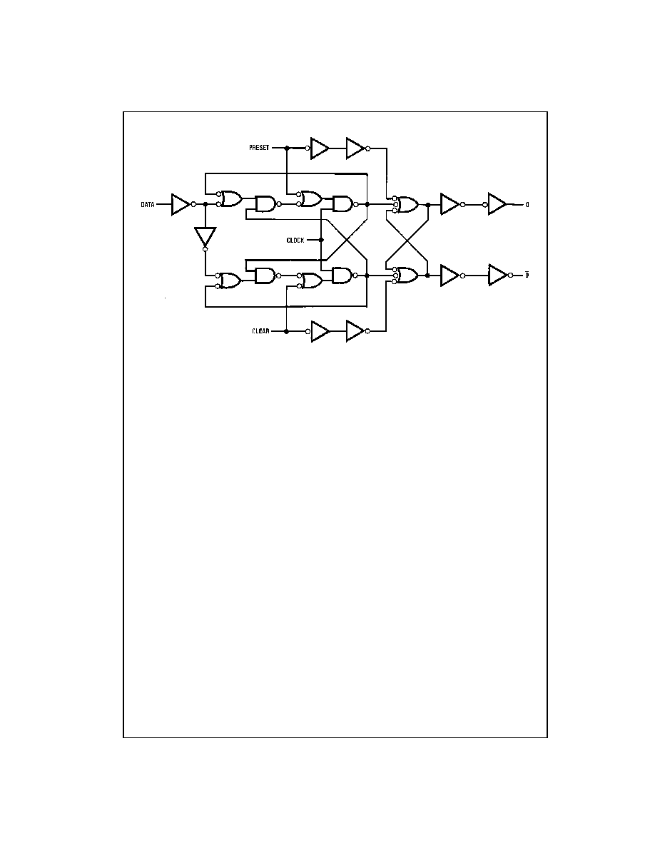
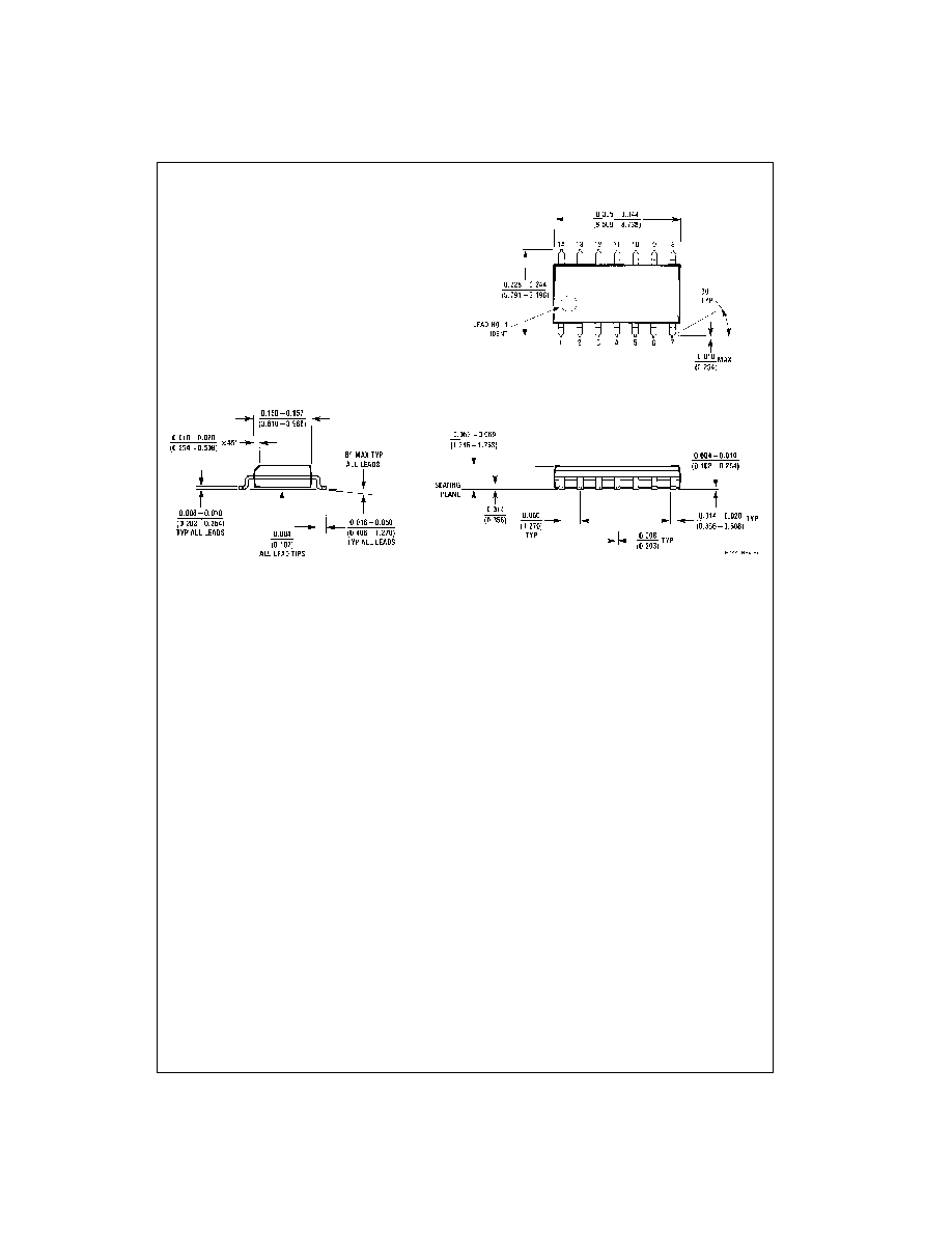
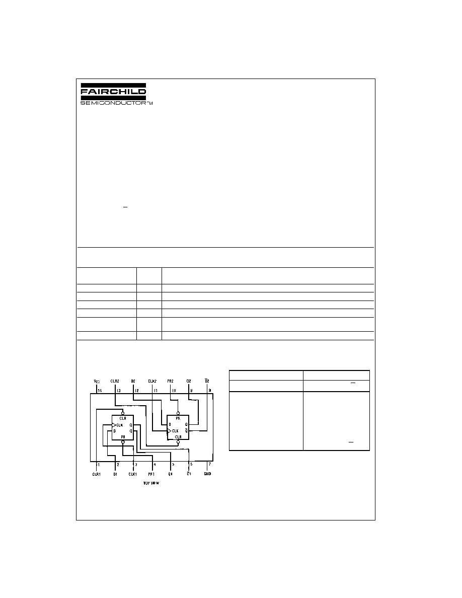
Connection Diagram
Pin Assignments for DIP, SOIC, SOP and TSSOP
Truth Table
Note: Q0
=
the level of Q before the indicated input conditions were estab-
lished.
Note 1: This configuration is nonstable; that is, it will not persist when pre-
set and clear inputs return to their inactive (HIGH) level.
Order Number
Package
Package Description
Number
MM74HC74AM
M14A
14-Lead Small Outline Integrated Circuit (SOIC), JEDEC MS-012, 0.150" Narrow
MM74HC74AMX_NL
M14A
Pb-Free 14-Lead Small Outline Integrated Circuit (SOIC), JEDEC MS-012, 0.150" Narrow
MM74HC74ASJ
M14D
Pb-Free 14-Lead Small Outline Package (SOP), EIAJ TYPE II, 5.3mm Wide
MM74HC74AMTC
MTC14
14-Lead Thin Shrink Small Outline Package (TSSOP), JEDEC MO-153, 4.4mm Wide
MM74HC74AMTCX_NL
MTC14
Pb-Free 14-Lead Thin Shrink Small Outline Package (TSSOP), JEDEC MO-153, 4.4mm
Wide
MM74HC74AN
N14A
14-Lead Plastic Dual-In-Line Package (PDIP), JEDEC MS-001, 0.300" Wide
Inputs
Outputs
PR
CLR
CLK
D
Q
Q
L
H
X
X
H
L
H
L
X
X
L
H
L
L
X
X
H (Note 1)
H (Note 1)
H
H
H
H
L
H
H
L
L
H
H
H
L
X
Q0
Q 0
3
www.fairchildsemi.com
MM74HC74A
Absolute Maximum Ratings
(Note 2)
(Note 3)
Recommended Operating
Conditions
Note 2: Absolute Maximum Ratings are those values beyond which dam-
age to the device may occur.
Note 3: Unless otherwise specified all voltages are referenced to ground.
Note 4: Power Dissipation temperature derating -- plastic "N" package:
-
12 mW/
∞
C from 65
∞
C to 85
∞
C.
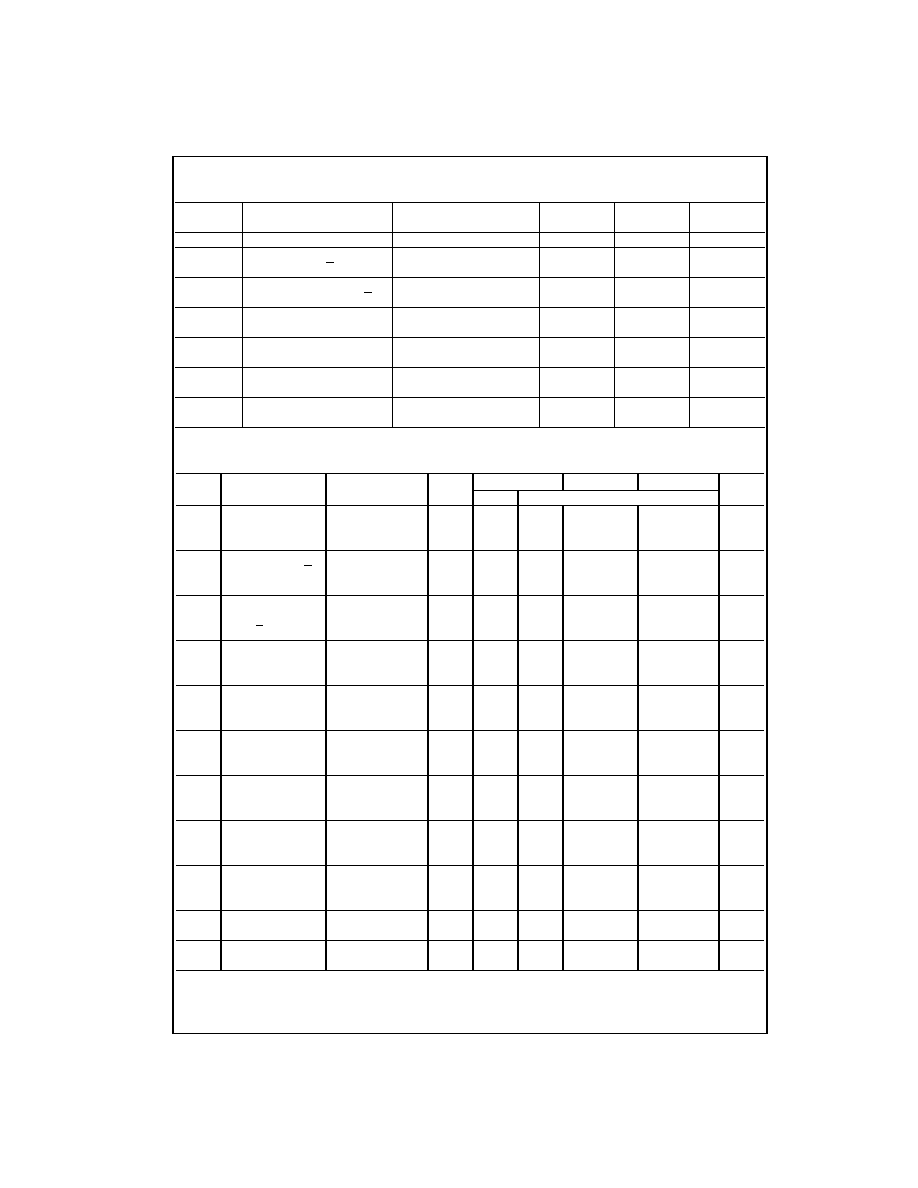
DC Electrical Characteristics
(Note 5)
Note 5: For a power supply of 5V
±
10% the worst case output voltages (V
OH
, and V
OL
) occur for HC at 4.5V. Thus the 4.5V values should be used when
designing with this supply. Worst case V
IH
and V
IL
occur at V
CC
=
5.5V and 4.5V respectively. (The V
IH
value at 5.5V is 3.85V.) The worst case leakage cur-
rent (I
IN
, I
CC
, and I
OZ
) occur for CMOS at the higher voltage and so the 6.0V values should be used.
Supply Voltage (V
CC
)
-
0.5 to
+
7.0V
DC Input Voltage (V
IN
)
-
1.5 to V
CC
+
1.5V
DC Output Voltage (V
OUT
)
-
0.5 to V
CC
+
0.5V
Clamp Diode Current (I
IK
, I
OK
)
±
20 mA
DC Output Current, per pin (I
OUT
)
±
25 mA
DC V
CC
or GND Current, per pin
(I
CC
)
±
50 mA
Storage Temperature Range (T
STG
)
-
65
∞
C to
+
150
∞
C
Power Dissipation (P
D
)
(Note 4)
600 mW
S.O. Package only
500 mW
Lead Temperature (T
L
)
(Soldering 10 seconds)
260
∞
C
Min
Max
Units
Supply Voltage (V
CC
)
2
6
V
DC Input or Output Voltage
0
V
CC
V
(V
IN
,
OUT
)
Operating Temperature Range (T
A
)
-
40
+
85
∞
C
Input Rise or Fall Times
(t
r
, t
f
) V
CC
=
2.0V
1000
ns
V
CC
=
4.5V
500
ns
V
CC
=
6.0V
400
ns
Symbol
Parameter
Conditions
V
CC
T
A
=
25
∞
C
T
A
=
-
40 to 85
∞
C T
A
=
-
55 to 125
∞
C
Units
Typ
Guaranteed Limits
V
IH
Minimum HIGH Level
2.0V
1.5
1.5
1.5
V
Input Voltage
4.5V
3.15
3.15
3.15
V
6.0V
4.2
4.2
4.2
V
V
IL
Maximum LOW Level
2.0V
0.5
0.5
0.5
V
Input Voltage
4.5V
1.35
1.35
1.35
V
6.0V
1.8
1.8
1.8
V
V
OH
Minimum HIGH Level
V
IN
=
V
IH
or V
IL
Output Voltage
|I
OUT
|
20
µ
A
2.0V
2.0
1.9
1.9
1.9
V
4.5V
4.5
4.4
4.4
4.4
V
6.0V
6.0
5.9
5.9
5.9
V
V
IN
=
V
IH
or V
IL
|I
OUT
|
4.0 mA
4.5V
4.3
3.98
3.84
3.7
V
|I
OUT
|
5.2 mA
6.0V
5.2
5.48
5.34
5.2
V
V
OL
Maximum LOW Level
V
IN
=
V
IH
or V
IL
Output Voltage
|I
OUT
|
20
µ
A
2.0V
0
0.1
0.1
0.1
V
4.5V
0
0.1
0.1
0.1
V
6.0V
0
0.1
0.1
0.1
V
V
IN
=
V
IH
or V
IL
|I
OUT
|
4.0 mA
4.5V
0.2
0.26
0.33
0.4
V
|I
OUT
|
5.2 mA
6.0V
0.2
0.26
0.33
0.4
V
I
IN
Maximum Input
V
IN
=
V
CC
or GND
6.0V
±
0.1
±
1.0
±
1.0
µ
A
Current
I
CC
Maximum Quiescent
V
I N
=
V
CC
or GND
6.0V
4.0
40
80
µ
A
Supply Current
I
OUT
=
0
µ
A
www.fairchildsemi.com
4
M
M
74
H
C
74
A
AC Electrical Characteristics
V
CC
=
5V, T
A
=
25
∞
C, C
L
=
15 pF, t
r
=
t
f
=
6 ns
AC Electrical Characteristics
C
L
=
50 pF, t
r
=
t
f
=
6 ns (unless otherwise specified)
Note 6: C
PD
determines the no load dynamic power consumption, P
D
=
C
PD
V
CC
2
f
+
I
CC
V
CC
, and the no load dynamic current consumption,
I
S
=
C
PD
V
CC
f
+
I
CC
.
Symbol
Parameter
Conditions
Typ
Guaranteed
Units
Limit
f
MAX
Maximum Operating Frequency
72
30
MHz
t
PHL
, t
PLH
Maximum Propagation
10
30
ns
Delay Clock to Q or Q
t
PHL
, t
PLH
Maximum Propagation
17
40
ns
Delay Preset or Clear to Q or Q
t
REM
Minimum Removal Time,
6
5
ns
Preset or Clear to Clock
t
s
Minimum Setup Time
10
20
ns
Data to Clock
t
H
Minimum Hold Time
0
0
ns
Clock to Data
t
W
Minimum Pulse Width
8
16
ns
Clock, Preset or Clear
Symbol
Parameter
Conditions
V
CC
T
A
=
25
∞
C
T
A
=
-
40 to 85
∞
C T
A
=
-
55 to 125
∞
C
Units
Typ
Guaranteed Limits
f
MAX
Maximum Operating
2.0V
22
6
5
4
MHz
Frequency
4.5V
72
30
24
20
MHz
6.0V
94
35
28
24
MHz
t
PHL
, t
PLH
Maximum Propagation
2.0V
34
110
140
165
ns
Delay Clock to Q or Q
4.5V
12
22
28
33
ns
6.0V
10
19
24
28
ns
t
PHL
, t
PLH
Maximum Propagation
2.0V
66
150
190
225
ns
Delay Preset or Clear
4.5V
20
30
38
45
ns
To Q or Q
6.0V
16
26
33
38
ns
t
REM
Minimum Removal Time
2.0V
20
50
65
75
ns
Preset or Clear
4.5V
6
10
13
15
ns
To Clock
6.0V
5
9
11
13
ns
t
s
Minimum Setup Time
2.0V
35
80
100
120
ns
Data to Clock
4.5V
10
16
20
24
ns
6.0V
8
14
17
20
ns
t
H
Minimum Hold Time
2.0V
0
0
0
ns
Clock to Data
4.5V
0
0
0
ns
6.0V
0
0
0
ns
t
W
Minimum, Pulse Width
2.0V
30
80
101
119
ns
Clock, Preset or Clear
4.5V
9
16
20
24
ns
6.0V
8
14
17
20
ns
t
TLH
, t
THL
Maximum Output
2.0V
25
75
95
110
ns
Rise and Fall Time
4.5V
7
15
19
22
ns
6.0V
6
13
16
19
ns
t
r
, t
f
Maximum Input Rise
2.0V
1000
1000
1000
ns
and Fall Time
4.5V
500
500
500
ns
6.0V
400
400
400
ns
C
PD
Power Dissipation
(per flip-flop)
80
pF
Capacitance (Note 6)
C
IN
Maximum Input
5
10
10
10
pF
Capacitance