February 1984
Revised February 1999
MM74HCT05 He
x In
ver
ter
(
O
pen
Dr
ain)
© 1999 Fairchild Semiconductor Corporation
DS005358.prf
www.fairchildsemi.com
MM74HCT05
Hex Inverter (Open Drain)
General Description
The MM74HCT05 is a logic function fabricated by using
advanced silicon-gate CMOS technology, which provides
the inherent benefits of CMOS--low quiescent power and
wide power supply range. The device is also input and out-
put characteristic and pinout compatible with standard
DM74LS logic families. The MM74HCT05 open drain Hex
Inverter requires the addition of an external resistor to per-
form a wire-NOR function.
All inputs are protected from static discharge damage by
internal diodes to V
CC
and ground.
MM74HCT devices are intended to interface between TTL
and NMOS components and standard CMOS devices.
These parts are also plug-in replacements for LS-TTL
devices and can be used to reduce power consumption in
existing designs.
Features
s
Open drain for wire-NOR function
s
LS-TTL pinout and threshold compatible
s
Fanout of 10 LS-TTL loads
s
Typical propagation delays:
t
PLH
(with 1 k
resistor) 10 ns
t
PHL
(with 1 k
resistor) 8 ns
Ordering Code:
Devices also available in Tape and Reel. Specify by appending the suffix letter "X" to the ordering code.
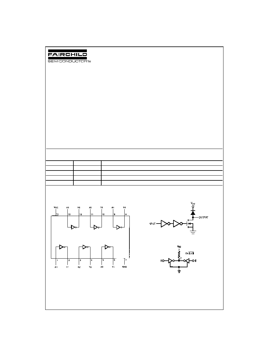
Connection Diagram
Pin Assignments for DIP, SOIC, SOP and TSSOP
Top View
Logic Diagram
Typical Application
Order Number
Package Number
Package Description
MM74HCT05M
M14A
14-Lead Small Outline Integrated Circuit (SOIC), JEDEC MS-120, 0.150" Narrow
MM74HCT05SJ
M14D
14-Lead Small Outline Package (SOP), EIAJ TYPE II, 5.3mm Wide
MM74HCT05MTC
MTC14
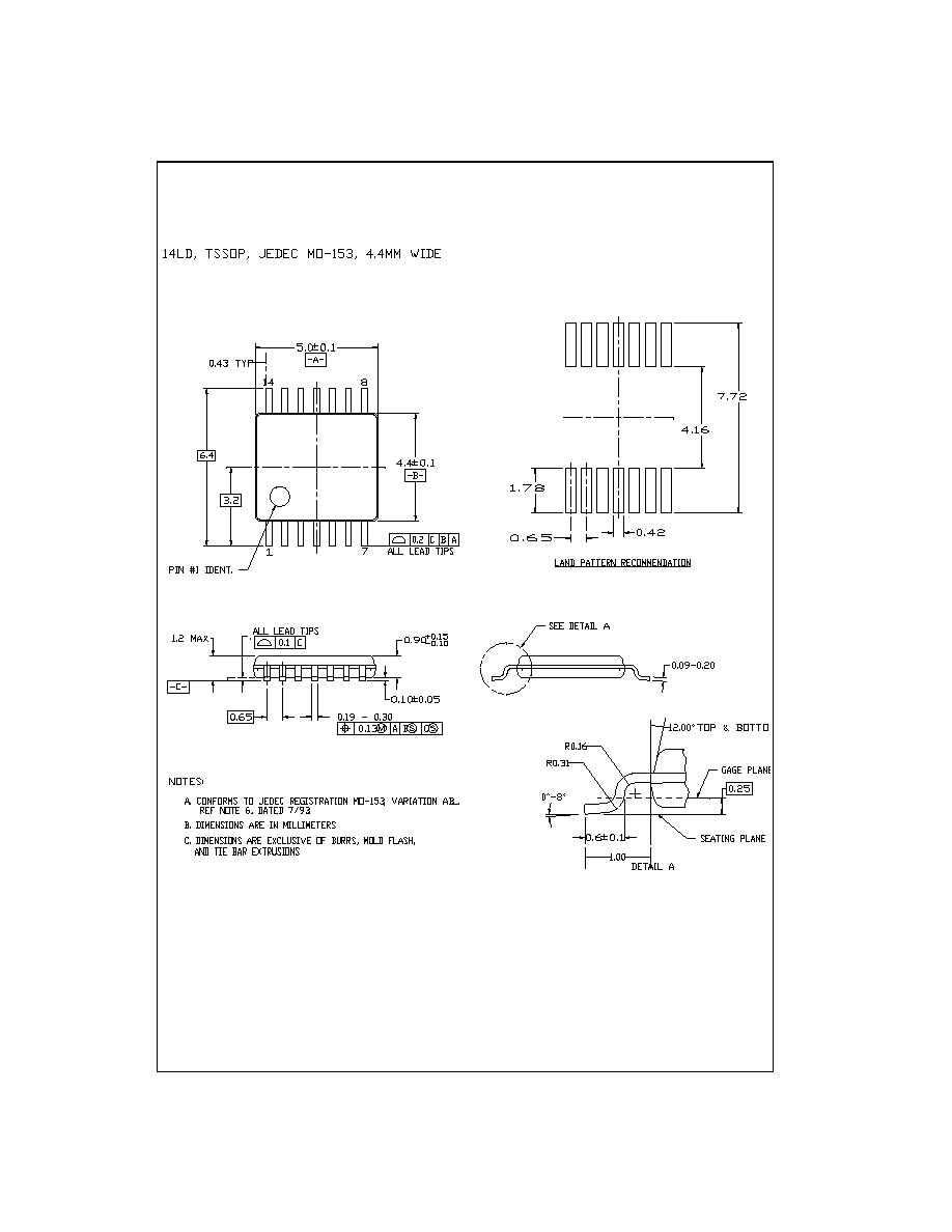
14-Lead Thin Shrink Small Outline Package (TSSOP), JEDEC MO-153, 4.4mm Wide
MM74HCT05N
N14A
14-Lead Plastic Dual-In-Line Package (PDIP), JEDEC MS-001, 0.300" Wide
www.fairchildsemi.com
2
MM
74
H
C
T05
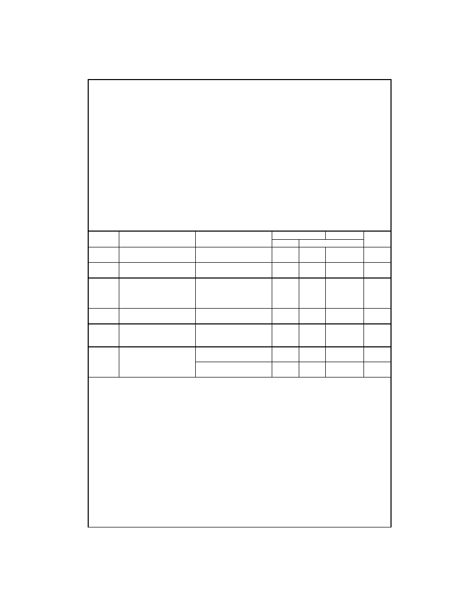
Absolute Maximum Ratings
(Note 1)
(Note 2)
Recommended Operating
Conditions
Note 1: Absolute Maximum Ratings are those values beyond which dam-
age to the device may occur.
Note 2: Unless otherwise specified all voltages are referenced to ground.
Note 3: Power Dissipation temperature derating -- plastic "N" package:
-
12 mW/
∞
C from 65
∞
C to 85
∞
C.
DC Electrical Characteristics
(V
CC
=
5V
±
10%,unless otherwise specified)
Note 4: This is measured per input with all other inputs held at V
CC
or ground.
Supply Voltage (V
CC
)
-
0.5 to
+
7.0V
DC Input Voltage (V
IN
)
-
1.5 to V
CC
+
1.5V
DC Output Voltage (V
OUT
)
-
0.5 to V
CC
+
0.5V
Clamp Diode Current (I
IK
, I
OK
)
±
20 mA
DC Output Current, per pin (I
OUT
)
±
25 mA
DC V
CC
or GND Current, per pin (I
CC
)
±
50 mA
Storage Temperature Range (T
STG
)
-
65
∞
C to
+
150
∞
C
Power Dissipation (P
D
)
(Note 3)
600 mW
S.O. Package only
500 mW
Lead Temperature (T
L
)
(Soldering 10 seconds)
260
∞
C
Min
Max
Units
Supply Voltage (V
CC
)
4.5
5.5
V
DC Input or Output Voltage
(V
IN
, V
OUT
)
0
V
CC
V
Operating Temperature Range (T
A
)
-
40
+
85
∞
C
Input Rise or Fall Times
(t
r
, t
f
)
500
ns
Symbol
Parameter
Conditions
T
A
=
25
∞
C
T
A
=
-
40 to 85
∞
C
Units
Typ
Guaranteed Limits
V
IH
Minimum HIGH Level
2.0
2.0
V
Input Voltage
V
IL
Maximum LOW Level
0.8
0.8
V
Input Voltage
V
OL
Maximum LOW
V
IN
=
V
IH
Level Voltage
|I
OUT
|
=
20
µ
A
0
0.1
0.1
V
|I
OUT
|
=
4.0 mA, V
CC
=
4.5V
0.2
0.26
0.33
V
|I
OUT
|
=
4.8 mA, V
CC
=
5.5V
0.2
0.26
0.33
V
I
IN
Maximum Input
V
IN
=
V
CC
or GND,
±
0.1
±
1.0
µ
A
Current
V
IH
or V
IL
I
LKG
Maximum HIGH Level
V
IN
=
V
IH
or VIL, V
OUT
=
V
CC
0.5
5.0
µ
A
Output Leakage
Current
I
CC
Maximum Quiescent
V
IN
=
V
CC
or GND
2.0
20
µ
A
Supply Current
I
OUT
=
0
µ
A
V
IN
=
2.4V or 0.5V
0.3
0.4
mA
(Note 4)
3
www.fairchildsemi.com
MM74HCT05
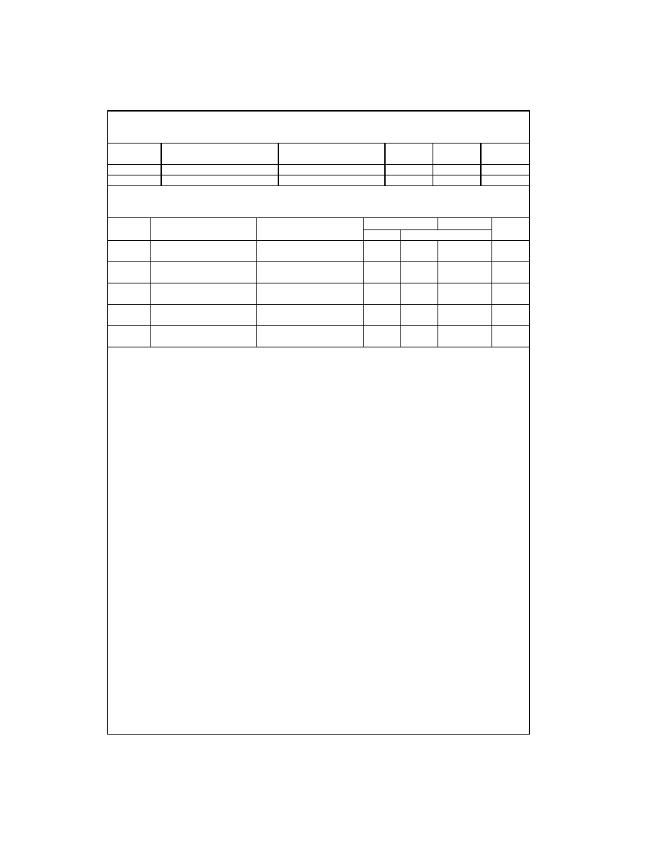
AC Electrical Characteristics
V
CC
=
5V, T
A
=
25
∞
C,C
L
=
15 pF, t
r
=
t
f
=
6 ns unless otherwise noted.
AC Electrical Characteristics
V
CC
=
5V,
±
10%, C
L
=
50pF, t
r
=
t
f
=
6ns unless otherwise specified.
Note 5: C
PD
determines the no load dynamic power consumption, P
D
=
C
PD
V
CC
2
f
+
I
CC
V
CC
, and the no load dynamic current consumption,
I
S
=
C
PD
V
CC
f
+
I
CC
.
Symbol
Parameter
Conditions
Typ
Guaranteed
Units
Limit
t
PZL
Maximum Propagation Delay
R
L
=
1 k
8
15
ns
t
PLZ
Maximum Propagation Delay
R
L
=
1 k
9
16
ns
Symbol
Parameter
Conditions
T
A
=
25
∞
C
T
A
=
-
40 to 85
∞
C
Units
Typ
Guaranteed Limits
t
PZL
Maximum Propagation
R
L
=
1k
10
22
28
ns
Delay
t
PLZ
Maximum Propagation
R
L
=
1 k
12
20
25
ns
Delay
t
THL
Maximum Output
10
15
19
ns
Fall Time
C
PD
Power Dissipation
(per gate)
20
pF
Capacitance (Note 5)
R
L
=
C
IN
Maximum Input
5
10
pF
Capacitance
www.fairchildsemi.com
4
MM
74
H
C
T05
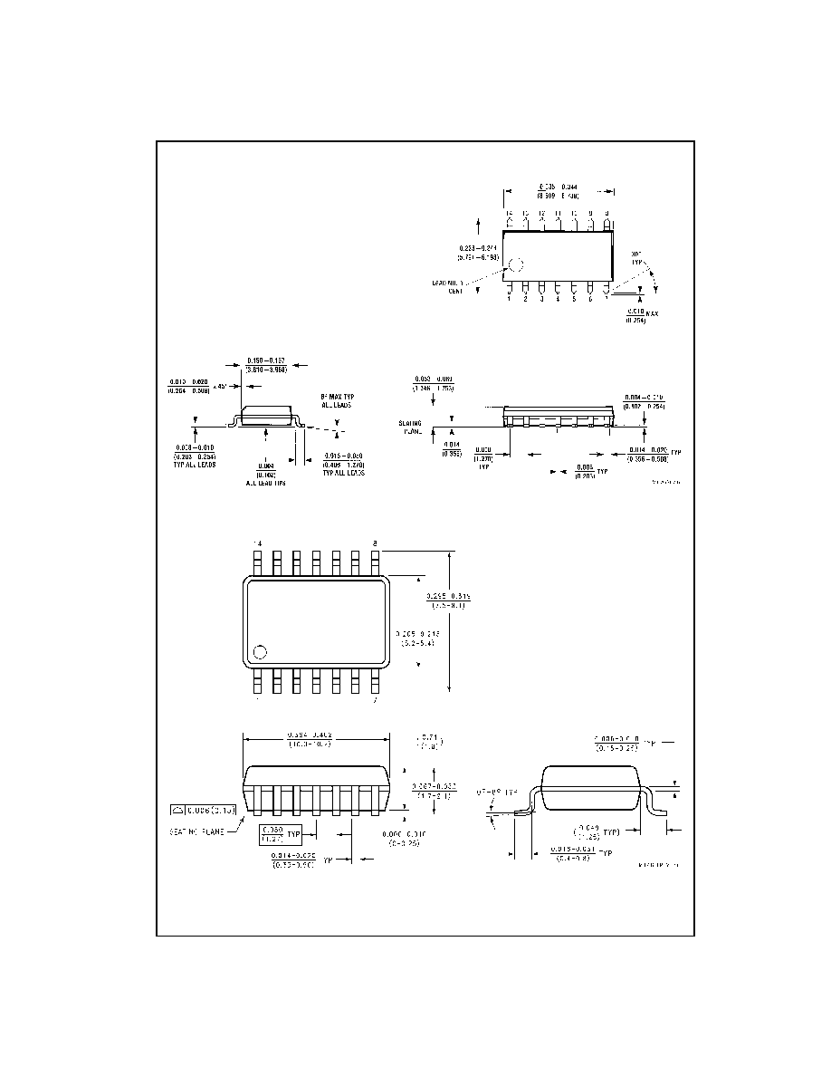
Physical Dimensions
inches (millimeters) unless otherwise noted
14-Lead Small Outline Integrated Circuit (SOIC), JEDEC MS-120, 0.150" Narrow
Package Number M14A
14-Lead Small Outline Package (SOP), EIAJ TYPE II, 5.3mm Wide
Package Number M14D
5
www.fairchildsemi.com
MM74HCT05
Physical Dimensions
inches (millimeters) unless otherwise noted (Continued)
14-Lead Thin Shrink Small Outline Package (TSSOP), JEDEC MO-153, 4.4mm Wide
Package Number MTC14
Fairchild does not assume any responsibility for use of any circuitry described, no circuit patent licenses are implied and Fairchild reserves the right at any time without notice to change said circuitry and specifications.
MM74HCT05 He
x I
n
ver
t
e
r
(
O
pen
Drai
n)
LIFE SUPPORT POLICY
FAIRCHILD'S PRODUCTS ARE NOT AUTHORIZED FOR USE AS CRITICAL COMPONENTS IN LIFE SUPPORT
DEVICES OR SYSTEMS WITHOUT THE EXPRESS WRITTEN APPROVAL OF THE PRESIDENT OF FAIRCHILD
SEMICONDUCTOR CORPORATION. As used herein:
1. Life support devices or systems are devices or systems
which, (a) are intended for surgical implant into the
body, or (b) support or sustain life, and (c) whose failure
to perform when properly used in accordance with
instructions for use provided in the labeling, can be rea-
sonably expected to result in a significant injury to the
user.
2. A critical component in any component of a life support
device or system whose failure to perform can be rea-
sonably expected to cause the failure of the life support
device or system, or to affect its safety or effectiveness.
www.fairchildsemi.com
Physical Dimensions
inches (millimeters) unless otherwise noted (Continued)
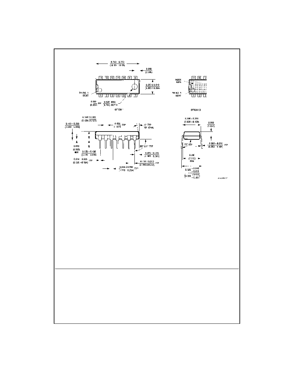
14-Lead Plastic Dual-In-Line Package (PDIP), JEDEC MS-001, 0.300" Wide
Package Number N14A