Äîêóìåíòàöèÿ è îïèñàíèÿ www.docs.chipfind.ru
February 1984
Revised January 1999
MM74HCT74 Dual D-T
ype Fli
p
-Fl
op w
i
th Pres
et and
Cl
ear
© 1999 Fairchild Semiconductor Corporation
DS005360.prf
www.fairchildsemi.com
MM74HCT74
Dual D-Type Flip-Flop with Preset and Clear
General Description
The MM74HCT74 utilizes advanced silicon-gate CMOS
technology to achieve operation speeds similar to the
equivalent LS-TTL part. It possesses the high noise immu-
nity and low power consumption of standard CMOS inte-
grated circuits, along with the ability to drive 10 LS-TTL
loads.
This flip-flop has independent data, preset, clear, and clock
inputs and Q and Q outputs. The logic level present at the
data input is transferred to the output during the positive-
going transition of the clock pulse. Preset and clear are
independent of the clock and accomplished by a low level
at the appropriate input.
The 74HCT logic family is functionally and pin-out compati-
ble with the standard 74LS logic family. All inputs are pro-
tected from damage due to static discharge by internal
diode clamps to V
CC
and ground.
MM74HCT devices are intended to interface between TTL
and NMOS components and standard CMOS devices.
These parts are also plug-in replacements for LS-TTL
devices and can be used to reduce power consumption in
existing designs.
Features
s
Typical propagation delay: 20 ns
s
Low quiescent current: 40
µ
A maximum (74HCT Series)
s
Low input current: 1
µ
A maximum
s
Fanout of 10 LS-TTL loads
s
Meta-stable hardened
Ordering Code:
Devices also available in Tape and Reel. Specify by appending the suffix letter "X" to the ordering code.
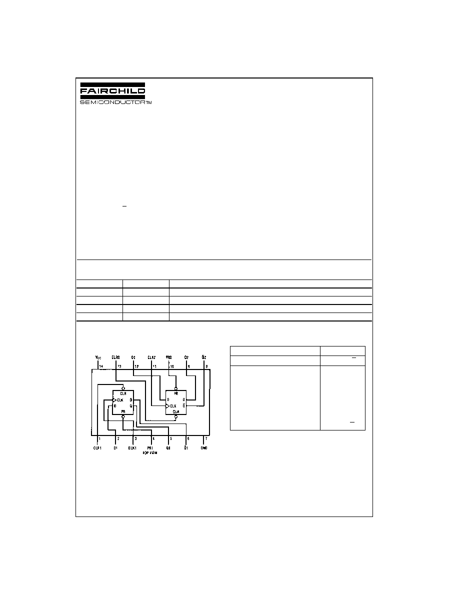
Connection Diagram
Pin Assignments for DIP, SOIC, SOP and TSSOP
Truth Table
Q0
=
the level of Q before the indicated input conditions were established.
Note 1: This configuration is nonstable; that is, it will not persist when pre-
set and clear inputs return to their inactive (HIGH) level.
Order Number
Package Number
Package Description
MM74HCT74M
M14A
14-Lead Small Outline Integrated Circuit (SOIC), JEDEC MS-120, 0.150" Narrow
MM74HCT74SJ
M14D
14-Lead Small Outline Package (SOP), EIAJ TYPE II, 5.3mm Wide
M74HCT74MTC
MTC14
14-Lead Thin Shrink Small Outline Package (TSSOP), JEDEC MO-153, 4.4mm Wide
MM74HCT74N
N14A
14-Lead Plastic Dual-In-Line Package (PDIP), JEDEC MS-001, 0.300" Wide
Inputs
Outputs
PR
CLR
CLK
D
Q
Q
L
H
X
X
H
L
H
L
X
X
L
H
L
L
X
X
H
(Note 1)
H
(Note 1)
H
H
H
H
L
H
H
L
L
H
H
H
L
X
Q0
Q0
www.fairchildsemi.com
2
MM
74
H
C
T74
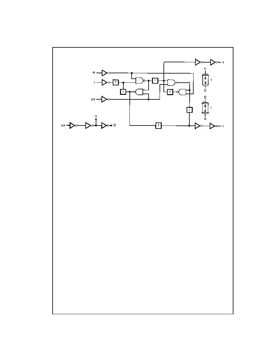
Logic Diagram
3
www.fairchildsemi.com
MM74HCT74
Absolute Maximum Ratings
(Note 2)
(Note 3)
Recommended Operating
Conditions
Note 2: Absolute Maximum Ratings are those values beyond which dam-
age to the device may occur.
Note 3: Unless otherwise specified all voltages are referenced to ground.
Note 4: Power Dissipation temperature derating -- plastic "N" package:
-
12 mW/
°
C from 65
°
C to 85
°
C.
DC Electrical Characteristics
V
CC
=
5V
±
10% (unless otherwise specified)
Note 5: This is measured per pin. All other inputs are held at V
CC
Ground.
Supply Voltage (V
CC
)
-
0.5 to
+
7.0V
DC Input Voltage (V
IN
)
-
1.5 to V
CC
+
1.5V
DC Output Voltage (V
OUT
)
-
0.5 to V
CC
+
0.5V
Clamp Diode Current (I
IK
, I
OK
)
±
20 mA
DC Output Current, per pin (I
OUT
)
±
25 mA
DC V
CC
or GND Current, per pin (I
CC
)
±
50 mA
Storage Temperature Range (T
STG
)
-
65
°
C to
+
150
°
C
Power Dissipation (P
D
)
(Note 4)
600 mW
S.O. Package only
500 mW
Lead Temperature (T
L
)
(Soldering 10 seconds)
260
°
C
Min
Max
Units
Supply Voltage (V
CC
)
4.5
5.5
V
DC Input or Output Voltage
(V
IN
, V
OUT
)
0
V
CC
V
Operating Temperature Range (T
A
)
-
40
+
85
°
C
Input Rise or Fall Times
(t
r
, t
f
)
500
ns
Symbol
Parameter
Conditions
T
A
=
25
°
C
T
A
=
-
40
°
to 85
°
C T
A
=
-
55 to 125
°
C
Units
Typ
Guaranteed Limits
V
IH
Minimum HIGH Level
2.0
2.0
2.0
V
Input Voltage
V
IL
Maximum LOW Level
0.8
0.8
0.8
V
Input Voltage
V
OH
Minimum HIGH Level
V
IN
=
V
IH
or V
IL
Output Voltage
|I
OUT
|
=
20
µ
A
V
CC
V
CC
-
0.1
V
CC
-
0.1
V
CC
-
0.1
V
|I
OUT
|
=
4.0 mA, V
CC
=
4.5V
4.2
3.98
3.84
3.7
V
|I
OUT
|
=
4.8 mA, V
CC
=
5.5V
5.2
4.98
4.84
4.7
V
V
OL
Maximum LOW Level
V
IN
=
V
IH
or V
IL
Voltage
|I
OUT
|
=
20
µ
A
0
0.1
0.1
0.1
V
|I
OUT
|
=
4.0 mA, V
CC
=
4.5V
0.2
0.26
0.33
0.4
V
|I
OUT
|
=
4.8 mA, V
CC
=
5.5V
0.2
0.26
0.33
0.4
V
I
IN
Maximum Input
V
IN
=
V
CC
or GND,
±
0.0.5
±
0.5
±
1.0
µ
A
Current
V
IH
or V
IL
I
CC
Maximum Quiescent
V
IN
=
V
CC
or GND
Supply Current
I
OUT
=
0
µ
A
2.0
20
80
µ
A
V
IN
=
2.4V or 0.5V (Note 5)
0.3
0.4
0.5
mA
www.fairchildsemi.com
4
MM
74
H
C
T74
AC Electrical Characteristics
V
CC
=
5V, T
A
=
25
°
C, C
L
=
15 pF, t
r
=
t
f
=
6 ns
AC Electrical Characteristics
V
CC
=
5.0V
±
10%, C
L
=
50 pF, t
r
=
t
f
=
6 ns unless otherwise specified
Note 6: C
PD
determines the no load dynamic power consumption, P
D
=
C
PD
V
CC
2
f
+
I
CC
V
CC
, and the no load dynamic current consumption,
I
S
=
C
PD
V
CC
f
+
I
CC
.
Symbol
Parameter
Conditions
Typ
Guaranteed
Units
Limit
f
MAX
Maximum Operating
50
30
MHz
Frequency from Clock
to Q or Q
t
PHL
, t
PLH
Maximum Propagation
18
30
ns
Delay Clock to Q or Q
t
PHL
, t
PLH
Maximum Propagation
18
30
ns
Delay from Preset or
Clear to Q or Q
t
REM
Minimum Removal Time,
20
ns
Preset or Clear to Clock
t
S
Minimum Setup Time
20
ns
Data to Clock
t
H
Minimum Hold Time
-
3
0
ns
Clock to Data
t
W
Minimum Pulse Width
8
16
ns
Clock, Preset or Clear
Symbol
Parameter
Conditions
T
A
=
25
°
C
T
A
=
-
40
°
to
+
85
°
C
Units
Typ
Guaranteed Limits
f
MAX
Maximum Operating
27
21
MHz
Frequency
t
PHL
, t
PLH
Maximum Propagation
21
35
44
ns
Delay from Clock to
Q or Q
t
PHL
, t
PLH
Maximum Propagation
21
35
44
ns
Delay from Preset or
Clear to Q or Q
t
REM
Minimum Removal Time
20
25
ns
Preset or Clear to Clock
t
S
Minimum Setup Time
20
25
ns
Data to Clock
t
H
Minimum Hold Time
-
3
0
0
ns
Clock to Data
t
W
Minimum Pulse Width
9
16
20
ns
Clock, Preset or Clear
t
r
, t
f
Maximum Clock Input
500
500
ns
Rise and Fall Time
t
THL
, t
TLH
Maximum Output
15
19
ns
Rise and Fall Time
C
PD
Power Dissipation
(per flip-flop)
10
pF
Capacitance (Note 6)
C
IN
Maximum Input
5
10
10
pF
Capacitance
5
www.fairchildsemi.com
MM74HCT74
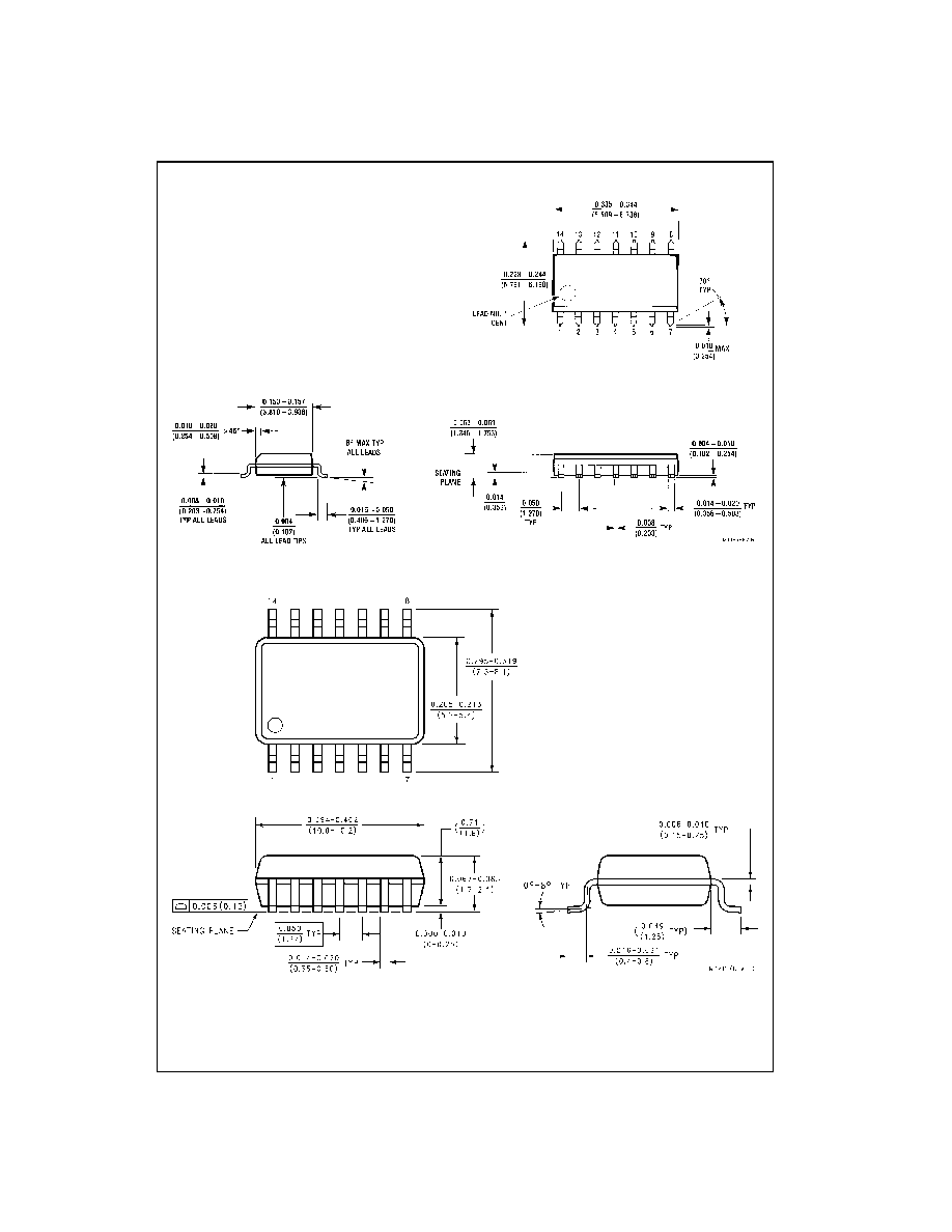
Physical Dimensions
inches (millimeters) unless otherwise noted
14-Lead Small Outline Integrated Circuit (SOIC), JEDEC MS-120, 0.150" Narrow
Package Number M14A
14-Lead Small Outline Package (SOP), EIAJ TYPE II, 5.3mm Wide
Package Number M14D
www.fairchildsemi.com
6
MM
74
H
C
T74
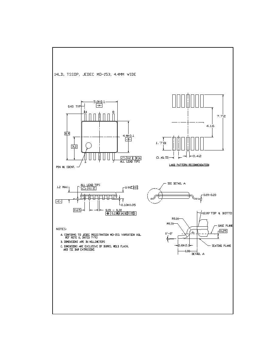
Physical Dimensions
inches (millimeters) unless otherwise noted (Continued)
14-Lead Thin Shrink Small Outline Package (TSSOP), JEDEC MO-153, 4.4mm Wide
Package Number MTC14
Fairchild does not assume any responsibility for use of any circuitry described, no circuit patent licenses are implied and Fairchild reserves the right at any time without notice to change said circuitry and specifications.
MM74HCT74 Dual D-T
ype Fli
p
-Fl
op w
i
th Pres
et and
Cl
ear
LIFE SUPPORT POLICY
FAIRCHILD'S PRODUCTS ARE NOT AUTHORIZED FOR USE AS CRITICAL COMPONENTS IN LIFE SUPPORT
DEVICES OR SYSTEMS WITHOUT THE EXPRESS WRITTEN APPROVAL OF THE PRESIDENT OF FAIRCHILD
SEMICONDUCTOR CORPORATION. As used herein:
1. Life support devices or systems are devices or systems
which, (a) are intended for surgical implant into the
body, or (b) support or sustain life, and (c) whose failure
to perform when properly used in accordance with
instructions for use provided in the labeling, can be rea-
sonably expected to result in a significant injury to the
user.
2. A critical component in any component of a life support
device or system whose failure to perform can be rea-
sonably expected to cause the failure of the life support
device or system, or to affect its safety or effectiveness.
www.fairchildsemi.com
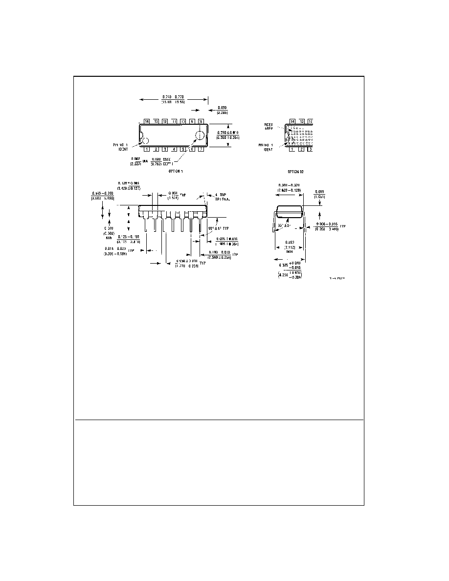
Physical Dimensions
inches (millimeters) unless otherwise noted (Continued)
14-Lead Plastic Dual-In-Line Package (PDIP), JEDEC MS-001, 0.300" Wide
Package Number N14A