 | –≠–ª–µ–∫—Ç—Ä–æ–Ω–Ω—ã–π –∫–æ–º–ø–æ–Ω–µ–Ω—Ç: MM80C97M | –°–∫–∞—á–∞—Ç—å:  PDF PDF  ZIP ZIP |
October 1987
Revised January 1999
MM80C95
∑
MM80C97 ∑
MM
8
0
C98
3-
ST
A
T
E He
x Buff
er
s
∑ 3-ST
A
T
E
He
x
I
n
ver
t
e
r
s
© 1999 Fairchild Semiconductor Corporation
DS005907.prf
www.fairchildsemi.com
MM80C95 ∑ MM80C97 ∑ MM80C98
3-STATE Hex Buffers ∑ 3-STATE Hex Inverters
General Description
The MM80C95, MM80C97 and MM80C98 gates are mono-
lithic complementary MOS (CMOS) integrated circuits con-
structed with N- and P-channel enhancement mode
transistors. The MM80C95 and the MM80C97 convert
CMOS or TTL outputs to 3-STATE outputs with no logic
inversion, the MM80C98 provides the logical opposite of
the input signal. The MM80C95 has common 3-STATE
controls for all six devices. The MM80C97 and the
MM80C98 have two 3-STATE controls; one for two devices
and one for the other four devices. Inputs are protected
from damage due to static discharge by diode clamps to
V
CC
and GND.
Features
s
Wide supply voltage range:
3.0V to 15V
s
Guaranteed noise margin:
1.0V
s
High noise immunity:
0.45 V
CC
(typ.)
s
TTL compatible:
Drive 1 TTL Load
Applications
∑ Bus drivers:
Typical propagation delay into 150 pF load
is 40 ns
Ordering Code:
Devices also available in Tape and Reel. Specify by appending the suffix letter "X" to the ordering code.
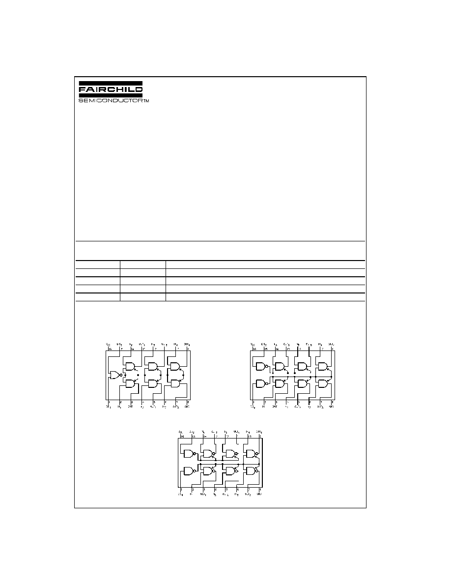
Connection Diagrams
Pin Assignments for DIP
MM80C95
Top View
MM80C97
Top View
MM80C98
Top View
Order Number
Package Number
Package Description
MM80C95N
N16E
16-Lead Plastic Dual-In-Line Package (PDIP), JEDEC MS-001, 0.300" Wide
MM80C97M
M16A
16-Lead Small Outline Integrated Circuit (SOIC), JEDEC MS-012, 0.150" Narrow
MM80C97N
N16E
16-Lead Plastic Dual-In-Line Package (PDIP), JEDEC MS-001, 0.300" Wide
MM80C98N
N16E
16-Lead Plastic Dual-In-Line Package (PDIP), JEDEC MS-001, 0.300" Wide
www.fairchildsemi.com
2
MM80C95
∑
MM80C97
∑ MM
80C98
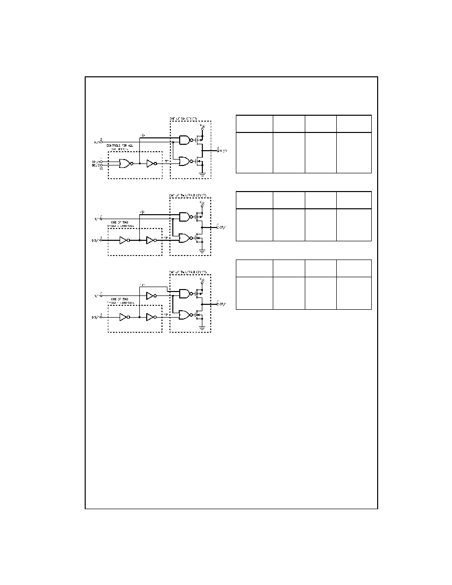
Schematic Diagrams
MM80C95 3-STATE
MM80C97 3-STATE
MM80C98 3-STATE
Truth Tables
MM80C95
MM80C97
MM80C98
X
=
Irrelevant
Note 1: Output 5≠6 only
Note 2: Output 1≠4 only
Disable
Input
Input
Output
DIS
1
DIS
2
0
0
0
0
0
0
1
1
0
1
X
H-z
1
0
X
H-z
1
1
X
H-z
Disable
Input
Input
Output
DIS
4
DIS
2
0
0
0
0
0
0
1
1
X
1
X
H-z (Note 1)
1
X
X
H-z (Note 2)
Disable
Input
Input
Output
DIS
4
DIS
2
0
0
0
1
0
0
1
0
X
1
X
H-z (Note 1)
1
X
X
H-z (Note 2)
3
www.fairchildsemi.com
MM80C95
∑
MM80C97 ∑
MM
8
0
C98
Absolute Maximum Ratings
(Note 3)
Note 3: "Absolute Maximum Ratings" are those values beyond which the
safety of the device cannot be guaranteed. Except for "Operating Tempera-
ture Range" they are not meant to imply that the device should be operated
at these limits. The table of "Electrical Characteristics" provides conditions
for actual device operation.
DC Electrical Characteristics
Min/Max limits apply across temperature range unless otherwise noted
Voltage at Any Pin
-
0.3V to V
CC
+
0.3V
Operating Temperature Range
-
40
∞
C to
+
85
∞
C
Storage Temperature Range
-
65
∞
C to
+
150
∞
C
Power Dissipation (P
D
)
Dual-In-Line
700 mW
Small Outline
500 mW
Power Supply Voltage (V
CC
)
18V
Lead Temperature
(Soldering, 10 seconds)
260
∞
C
Symbol
Parameter
Conditions
Min
Typ
Max
Units
CMOS TO CMOS
V
IN(1)
Logical "1" Input Voltage
V
CC
=
5V
3.5
V
V
CC
=
10V
8.0
V
V
IN(0)
Logical "0" Input Voltage
V
CC
=
5V
1.5
V
V
CC
=
10V
2.0
V
V
OUT(1)
Logical "1" Output Voltage
V
CC
=
5V
4.5
V
V
CC
=
10V
9.0
V
V
OUT(0)
Logical "0" Output Voltage
V
CC
=
5V
0.5
V
V
CC
=
10V
1.0
V
I
IN(1)
Logical "1" Input Current
V
CC
=
15V
0.005
1.0
µ
A
I
IN(0)
Logical "0" Input Current
-
1.0
-
0.005
µ
A
I
OZ
Output Current in High
V
CC
=
15V, V
O
=
15V
0.005
1.0
µ
A
Impedance State
V
CC
=
15V, V
O
=
0V
-
1.0
-
0.005
µ
A
I
CC
Supply Current
V
CC
=
15V
0.01
15
µ
A
TTL INTERFACE
V
IN(1)
Logical "1" Input Voltage
V
CC
=
4.75V
V
CC
-
1.5
V
V
IN(0)
Logical "0" Input Voltage
V
CC
=
4.75V
0.8
V
V
OUT(1)
Logical "1" Output Voltage
V
CC
=
4.75V,
2.4
V
I
O
=
-
1.6 mA
V
OUT(0)
Logical "0" Output Voltage
V
CC
=
4.75V,
0.4
V
I
O
=
1.6 mA
OUTPUT DRIVE (Short Circuit Current)
I
SOURCE
Output Source Current
V
CC
=
5V, V
IN(1)
=
5V
-
4.35
mA
T
A
=
25
∞
C, V
OUT
=
0V
I
SOURCE
Output Source Current
V
CC
=
10V, V
IN(1)
=
10V
-
20
mA
T
A
=
25
∞
C, V
OUT
=
0V
I
SINK
Output Sink Current
V
CC
=
5V, V
IN(0)
=
0V
4.35
mA
T
A
=
25
∞
C, V
OUT
=
V
CC
I
SINK
Output Sink Current
V
CC
=
10V, V
IN(0)
=
0V
20
mA
T
A
=
25
∞
C, V
OUT
=
V
CC
www.fairchildsemi.com
4
MM80C95
∑
MM80C97
∑ MM
80C98
AC Electrical Characteristics
(Note 4)
T
A
=
25
∞
C, C
L
=
50 pF, unless otherwise noted.
Note 4: AC Parameters are guaranteed by DC correlated testing.
Note 5: Capacitance is guaranteed by periodic testing.
Note 6: C
PD
determines the no load AC power consumption of any CMOS device. For complete explanation see Family Characteristics application note
AN-90.
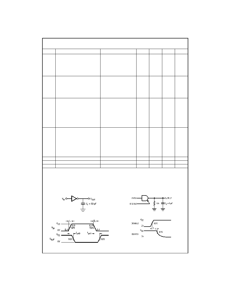
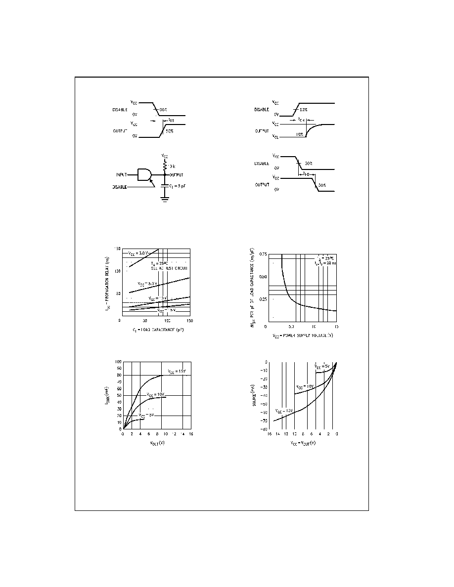
AC Test Circuits and Switching Time Waveforms
t
pd0,
t
pd1
CMOS to CMOS
t
1H
and t
H1
t
1H
Symbol
Parameter
Conditions
Min
Typ
Max
Units
t
pd0
, t
pd1
Propagation Delay Time to a Logical "0" or
Logical "1" from Data Input to Output
MM80C95, MM80C97
V
CC
=
5V
60
100
ns
V
CC
=
10V
25
40
ns
MM80C98
V
CC
=
5V
70
150
ns
V
CC
=
10V
35
75
ns
t
pd0
, t
pd1
Propagation Delay Time to a Logical "0" or
Logical "1" from Data Input to Output
MM80C95, MM80C97
V
CC
=
5V, C
L
=
150 pF
85
160
ns
V
CC
=
10V, C
L
=
150 pF
40
80
ns
MM80C98
V
CC
=
5V, C
L
=
150 pF
95
210
ns
V
CC
=
10V, C
L
=
150 pF
45
110
ns
t
1H
, t
0H
Delay from Disable Input to High Impedance R
L
=
10k, C
L
=
5 pF
State, (from Logical "1" or Logical "0")
MM80C95
V
CC
=
5V
80
135
ns
V
CC
=
10V
50
90
ns
MM80C97
V
CC
=
5V
70
125
ns
V
CC
=
10V
50
90
ns
MM80C98
V
CC
=
5V
90
170
ns
V
CC
=
10V
70
125
ns
t
H1
, t
H0
Delay from Disable Input to Logical "1" Level R
L
=
10k, C
L
=
50 pF
(from High Impedance State)
MM80C95
V
CC
=
5V
120
200
ns
V
CC
=
10V
50
90
ns
MM80C96
V
CC
=
5V
130
225
ns
V
CC
=
10V
60
110
ns
MM80C98
V
CC
=
5V
120
200
ns
V
CC
=
10V
50
90
ns
C
IN
Input Capacitance
Any Input (Note 5)
5.0
pF
C
OUT
Output Capacitance 3-STATE
Any Output (Note 5)
11
pF
C
PD
Power Dissipation Capacitance
(Note 6)
60
pF
5
www.fairchildsemi.com
MM80C95
∑
MM80C97 ∑
MM
8
0
C98
AC Test Circuits and Switching Time Waveforms
(Continued)
t
H1
t
0H
and t
H0
t
0H
t
H0
Note: Delays measured with input t
r
, t
f
20 ns.
Typical Performance Characteristics
Propagation Delay vs Load Capacitance
t
pd
/pF vs Power Supply Voltage
N-Channel Output Drive at 25
∞
C
P-Channel Output Drive at 25
∞
C