 | –≠–ª–µ–∫—Ç—Ä–æ–Ω–Ω—ã–π –∫–æ–º–ø–æ–Ω–µ–Ω—Ç: MM88C29N | –°–∫–∞—á–∞—Ç—å:  PDF PDF  ZIP ZIP |
October 1987
Revised January 1999
MM88C29
∑
MM88C30 Q
uad Si
ngle-
Ended Line Dri
ver ∑
Dual
Di
ff
erent
i
a
l Line Dri
ver
© 1999 Fairchild Semiconductor Corporation
DS005908.prf
www.fairchildsemi.com
MM88C29 ∑ MM88C30
Quad Single-Ended Line Driver ∑
Dual Differential Line Driver
General Description
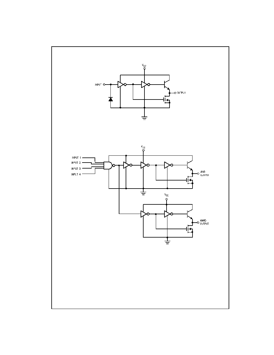
The MM88C30 is a dual differential line driver that also per-
forms the dual four-input NAND or dual four-input AND
function. The absence of a clamp diode to V
CC
in the input
protection circuitry of the MM88C30 allows a CMOS user to
interface systems operating at different voltage levels.
Thus, a CMOS digital signal source can operate at a V
CC
voltage greater than the V
CC
voltage of the MM88C30 line
driver. The differential output of the MM88C30 eliminates
ground-loop errors.
The MM88C29 is a non-inverting single-wire transmission
line driver. Since the output ON resistance is a low 20
typ., the device can be used to drive lamps, relays, sole-
noids, and clock lines, besides driving data lines.
Features
s
Wide supply voltage range:
3V to 15V
s
High noise immunity:
0.45 V
CC
(typ.)
s
Low output ON resistance:
20
(typ.)
Ordering Code:
Devices also available in Tape and Reel. Specify by appending suffix letter "X" to the ordering code.
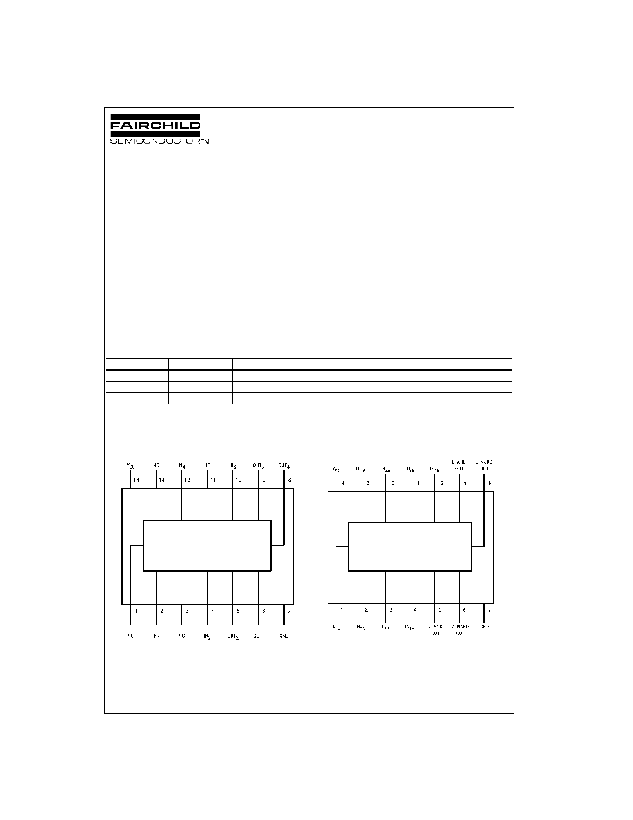
Connection Diagrams
Pin Assignments for DIP
MM88C29
Top View
Pin Assignments for DIP and SOIC
MM88C30
Top View
Order Number
Package Number
Package Description
MM88C29N
N14A
14-Lead Plastic Dual-In-Line Package (PDIP), JEDEC MS-001, 0.300" Wide
MM88C30M
M14A
14-Lead Small Outline Integrated Circuit (SOIC), JEDEC MS-120, 0.150" Narrow
MM88C30N
N14A
14-Lead Plastic Dual-In-Line Package (PDIP), JEDEC MS-001, 0.300" Wide
www.fairchildsemi.com
2
MM88C29
∑ MM
88C30
Logic Diagrams
1/4 MM88C29
1/2 MM88C30
3
www.fairchildsemi.com
MM88C29
∑ MM88C30
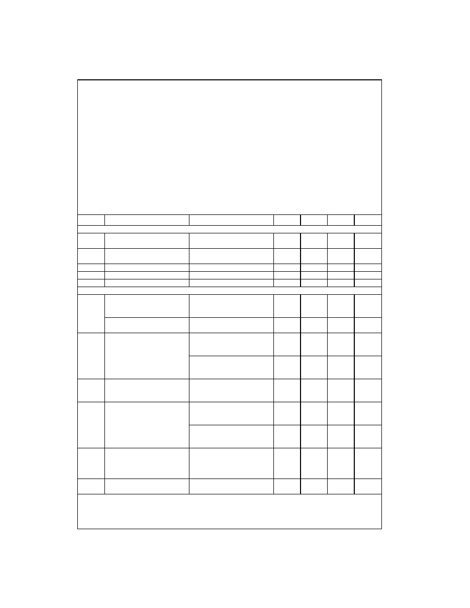
Absolute Maximum Ratings
(Note 1)
Note 1: "Absolute Maximum Ratings" are those values beyond which the
safety of the device cannot be guaranteed. Except for "Operating Tempera-
ture Range" they are not meant to imply that the devices should be oper-
ated at these limits. The Electrical Characteristics tables provide conditions
for actual device operation.
Note 2: AC Parameters are guaranteed by DC correlated testing.
DC Electrical Characteristics
Min/Max limits apply across temperature range unless otherwise noted
Voltage at Any Pin (Note 2)
-
0.3V to V
CC
+
16V
Operating Temperature Range
-
40
∞
C to
+
85
∞
C
Storage Temperature
-
65
∞
C to
+
150
∞
C
Power Dissipation (P
D
)
Dual-In-Line
700 mW
Small Outline
500 mW
Operating V
CC
Range
3V to 15V
Absolute Maximum V
CC
18V
Average Current at Output
MM88C30
50 mA
MM88C29
25 mA
Maximum Junction Temperature, T
j
150
∞
C
Lead Temperature
(Soldering, 10 seconds)
260
∞
C
Symbol
Parameter
Conditions
Min
Typ
Max
Units
CMOS TO CMOS
V
IN(1)
Logical "1" Input Voltage
V
CC
=
5V
3.5
V
V
CC
=
10V
8
V
V
IN(0)
Logical "0" Input Voltage
V
CC
=
5V
1.5
V
V
CC
=
10V
2
V
I
IN(1)
Logical "1" Input Current
V
CC
=
15V, V
IN
=
15V
0.005
1
µ
A
I
IN(0)
Logical "0" Input Current
V
CC
=
15V, V
IN
=
0V
-
1
-
0.005
µ
A
I
CC
Supply Current
V
CC
=
5V
0.05
100
mA
OUTPUT DRIVE
I
SOURCE
Output Source Current
V
OUT
=
V
CC
-
1.6V,
V
CC
4.75V, T
j
=
25
∞
C
-
47
-
80
mA
T
j
=
85
∞
C
-
32
-
60
mA
MM88C29
V
OUT
=
V
CC
-
0.8V
-
2
-
20
mA
MM88C30
V
CC
4.5V
I
SINK
Output Sink Current
V
OUT
=
0.4V, V
CC
=
4.75V,
T
j
=
25
∞
C
9.5
22
mA
T
j
=
85
∞
C
8
18
mA
V
OUT
=
0.4V, V
CC
=
10V,
T
j
=
25
∞
C
19
40
mA
T
j
=
125
∞
C
15.5
33
mA
I
SOURCE
Output Source Resistance
V
OUT
=
V
CC
-
1.6V,
V
CC
4.75V, T
j
=
25
∞
C
20
34
T
j
=
85
∞
C
27
50
I
SINK
Output Sink Resistance
V
OUT
=
0.4V, V
CC
=
4.75V,
T
j
=
25
∞
C
18
41
T
j
=
85
∞
C
22
50
V
OUT
=
0.4V, V
CC
=
10V,
T
j
=
25
∞
C
10
21
T
j
=
85
∞
C
12
26
Output Resistance
Temperature Coefficient
Source
0.55
%/
∞
C
Sink
0.40
%/
∞
C
JA
Thermal Resistance
150
∞
C/W
(N-Package)

www.fairchildsemi.com
4
MM88C29
∑ MM
88C30
AC Electrical Characteristics
(Note 2)
T
A
=
25
∞
C, C
L
=
50 pF
Note 3: Capacitance is guaranteed by periodic testing.
Note 4: C
PD
determines the no load AC power consumption of any CMOS device. For complete explanation see Family Characteristics application note
AN-90 (CMOS Logic Databook).
AC Test Circuits
FIGURE 1.
FIGURE 2.
Symbol
Parameter
Conditions
Min
Typ
Max
Units
t
pd
Propagation Delay Time to
Logical "1" or "0"
(See Figure 1)
MM88C29
V
CC
=
5V
80
200
ns
V
CC
=
10V
35
100
ns
MM88C30
V
CC
=
5V
110
350
ns
V
CC
=
10V
50
150
ns
t
pd
Differential Propagation Delay
R
L
=
100
, C
L
=
5000 pF
Time to Logical "1" or "0"
(See Figure 2)
MM88C30
V
CC
=
5V
400
ns
V
CC
=
10V
150
ns
C
IN
Input Capacitance
MM88C29
(Note 3)
5.0
pF
MM88C30
(Note 3)
5.0
pF
C
PD
Power Dissipation Capacitance
MM88C29
(Note 3)
150
pF
MM88C30
(Note 3)
200
pF

5
www.fairchildsemi.com
MM88C29
∑ MM88C30
Typical Applications
Digital Data Transmission
Note A: Exact value depends on line length.
Note B: Optional to control response time.
Note C: V
CC
=
4.5V to 5.5V for the DS7820, V
CC
=
4.5V to 15V for the DS78C20.
V
CC
is 3V to 15V.
Typical Data Rate vs Transmission Line Length
Note: The transmission line used was #22 gauge unshielded twisted pair
(40k termination).
Note: The curves generated assume that both drivers are driving equal
lines, and that the maximum power is 500 mW/package.
www.fairchildsemi.com
6
MM88C29
∑ MM
88C30
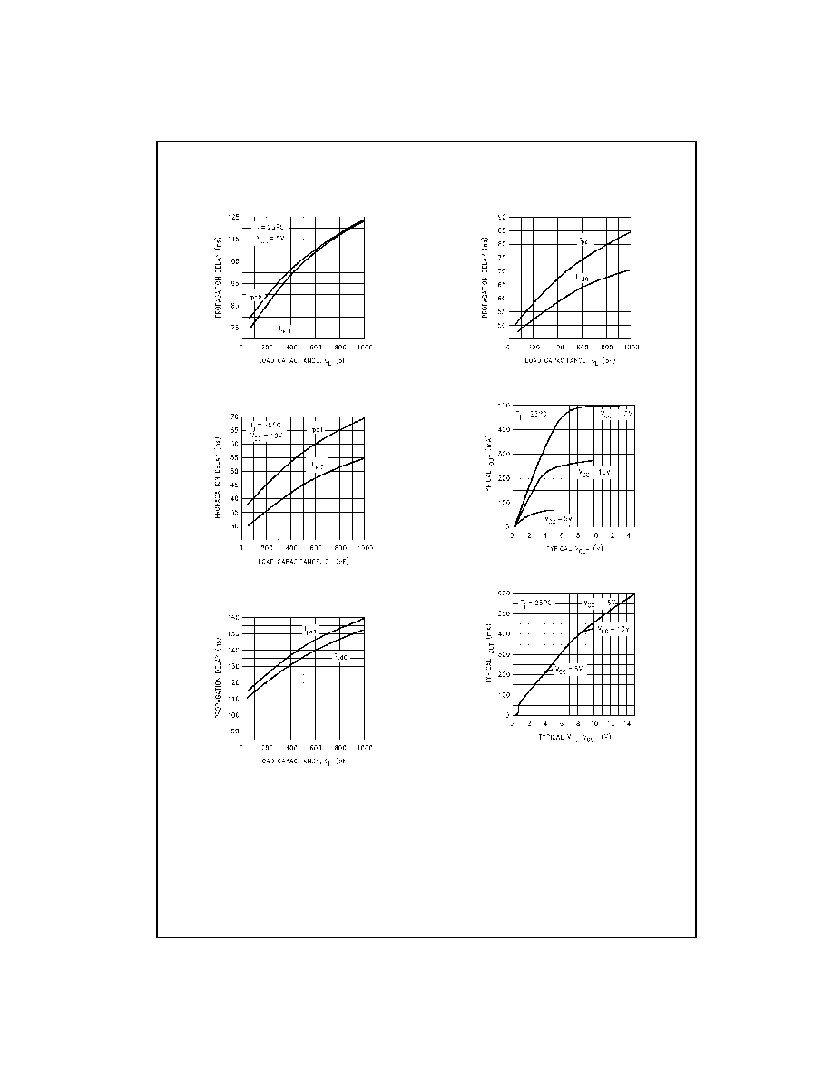
Typical Performance Characteristics
MM88C29
Typical Propagation Delay
vs Load Capacitance
MM88C29
Typical Propagation Delay
vs Load Capacitance
MM88C30
Typical Propagation Delay
vs Load Capacitance
MM88C30
Typical Propagation Delay
vs Load Capacitance
Typical Sink Current vs
Output Voltage
Typical Source Current
vs Output Voltage

7
www.fairchildsemi.com
MM88C29
∑ MM88C30
Physical Dimensions
inches (millimeters) unless otherwise noted
14-Lead Small Outline Integrated Circuit (SOIC), JEDEC MS-120, 0.150" Narrow
Package Number M14A

Fairchild does not assume any responsibility for use of any circuitry described, no circuit patent licenses are implied and Fairchild reserves the right at any time without notice to change said circuitry and specifications.
M
M
88C29
∑
MM88C30 Q
u
a
d
Singl
e-Ended Li
ne Dr
iver
∑
Dual D
iffer
e
nt
ial
Li
n
e
Dr
iver
LIFE SUPPORT POLICY
FAIRCHILD'S PRODUCTS ARE NOT AUTHORIZED FOR USE AS CRITICAL COMPONENTS IN LIFE SUPPORT
DEVICES OR SYSTEMS WITHOUT THE EXPRESS WRITTEN APPROVAL OF THE PRESIDENT OF FAIRCHILD
SEMICONDUCTOR CORPORATION. As used herein:
1. Life support devices or systems are devices or systems
which, (a) are intended for surgical implant into the
body, or (b) support or sustain life, and (c) whose failure
to perform when properly used in accordance with
instructions for use provided in the labeling, can be rea-
sonably expected to result in a significant injury to the
user.
2. A critical component in any component of a life support
device or system whose failure to perform can be rea-
sonably expected to cause the failure of the life support
device or system, or to affect its safety or effectiveness.
www.fairchildsemi.com
Physical Dimensions
inches (millimeters) unless otherwise noted (Continued)
14-Lead Plastic Dual-In-Line Package (PDIP), JEDEC MS-001, 0.300" Wide
Package Number N14A