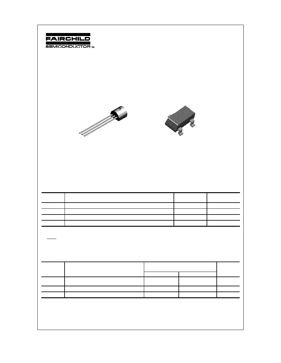
PN4091
PN4092
PN4093
MMBF4091
MMBF4092
MMBF4093
N-Channel Switch
This device is designed for low level analog switching, sample
and hold circuits and chopper stabalized amplifiers. Sourced
from Process 51. See J111 for characteristics.
Absolute Maximum Ratings*
TA = 25°C unless otherwise noted
*
These ratings are limiting values above which the serviceability of any semiconductor device may be impaired.
NOTES:
1) These ratings are based on a maximum junction temperature of 150 degrees C.
2) These are steady state limits. The factory should be consulted on applications involving pulsed or low duty cycle operations
Thermal Characteristics
TA = 25°C unless otherwise noted
Symbol
Parameter
Value
Units
V
DG
Drain-Gate Voltage
40
V
V
GS
Gate-Source Voltage
- 40
V
I
GF
Forward Gate Current
50
mA
T
J
,T
stg
Operating and Storage Junction Temperature Range
-55 to +150
°
C
Symbol
Characteristic
Max
Units
PN4091-4093
*MMBF4091-4093
P
D
Total Device Dissipation
Derate above 25
°
C
625
5.0
350
2.8
mW
mW/
°
C
R
JC
Thermal Resistance, Junction to Case
125
°
C/W
R
JA
Thermal Resistance, Junction to Ambient
357
556
°
C/W
G
S
D
TO-92
SOT-23
Mark: 61J / 61K / 61L
G
S
D
*
Device mounted on FR-4 PCB 1.6" X 1.6" X 0.06."
1997 Fairchild Semiconductor Corporation
NOTE: Source & Drain
are interchangeable
PN4091 / 4092 / 4093 / MMBF4091 / 4092 / 4093
5
Electrical Characteristics
TA = 25°C unless otherwise noted
Symbol
Parameter
Test Conditions
Min
Max
Units
OFF CHARACTERISTICS
ON CHARACTERISTICS
I
DSS
Zero-Gate Voltage Drain Current*
V
DS
= 20 V, V
GS
= 0
4091
4092
4093
30
15
8.0
mA
mA
mA
V
DS(
on
)
Drain-Source On Voltage
I
D
=
6.6 mA, V
GS
= 0
4091
I
D
=
4.0 mA, V
GS
= 0
4092
I
D
=
2.5 mA, V
GS
= 0
4093
0.2
0.2
0.2
V
V
V
r
DS(
on
)
Drain-Source On Resistance
I
D
=
1.0 mA, V
GS
= 0
4091
4092
4093
30
50
80
SMALL-SIGNAL CHARACTERISTICS
r
ds(on)
Drain-Source On Resistance
V
DS
= V
GS
= 0, f= 1.0 kHz 4091
4092
4093
30
50
80
C
iss
Input Capacitance
V
DS
= 20, V
GS
= 0, f = 1.0 MHz
16
pF
C
rss
Reverse Transfer Capacitance
V
GS
= - 20 V, f = 1.0 MHz
5.0
pF
SWITCHING CHARACTERISTICS
t
on
Turn-On Time
I
D(
on)
= 12 mA
4091
I
D(
on)
= 6.0 mA 4092
I
D(
on)
= 3.0 mA
4093
25
35
60
ns
ns
ns
t
off
Turn-Off Time
V
GS(
off)
= 12 V
4091
V
GS(
off)
= 6.0 V 4092
V
GS(
off)
= 3.0 V
4093
40
60
80
ns
ns
ns
*
Pulse Test: Pulse Width
300
µ
s, Duty Cycle
1.0%
V
(BR)GSS
Gate-Source Breakdown Voltage
I
G
= 1.0
µ
A, V
DS
= 0
- 40
V
V
GS(off)
Gate-Source Cutoff Voltage
V
DS
= 20 V, I
D
= 1.0 nA
4091
4092
4093
- 5.0
- 2.0
- 1.0
- 10
- 7.0
- 5.0
V
V
V
I
DGO
Drain-Gate Leakage Current
V
DG
= 20 V, I
S
= 0
V
DG
= 20 V, I
S
= 0, T
A
= 150
°
C
- 200
- 400
pA
nA
I
D(off)
Drain Cutoff Leakage Current
V
DS
= 20 V, V
GS
= - 12 V
4091
V
DS
= 20 V, V
GS
= - 8.0 V 4092
V
DS
= 20 V, V
GS
= - 6.0 V 4093
V
DS
= 20 V, V
GS
= -12 V,
T
A
= 150
°
C
4091
V
DS
= 20 V, V
GS
= - 8.0 V,
T
A
= 150
°
C
4092
V
DS
= 20 V, V
GS
= - 6.0 V,
T
A
= 150
°
C
4093
200
200
200
400
400
400
pA
pA
pA
nA
nA
nA
N-Channel Switch
(continued)
PN4091 / 4092 / 4093 / MMBF4091 / 4092 / 4093
TRADEMARKS
The following are registered and unregistered trademarks Fairchild Semiconductor owns or is authorized to use and is
not intended to be an exhaustive list of all such trademarks.
LIFE SUPPORT POLICY
FAIRCHILD'S PRODUCTS ARE NOT AUTHORIZED FOR USE AS CRITICAL COMPONENTS IN LIFE SUPPORT
DEVICES OR SYSTEMS WITHOUT THE EXPRESS WRITTEN APPROVAL OF FAIRCHILD SEMICONDUCTOR CORPORATION.
As used herein:
1. Life support devices or systems are devices or
systems which, (a) are intended for surgical implant into
the body, or (b) support or sustain life, or (c) whose
failure to perform when properly used in accordance
with instructions for use provided in the labeling, can be
reasonably expected to result in significant injury to the
user.
2. A critical component is any component of a life
support device or system whose failure to perform can
be reasonably expected to cause the failure of the life
support device or system, or to affect its safety or
effectiveness.
PRODUCT STATUS DEFINITIONS
Definition of Terms
Datasheet Identification
Product Status
Definition
Advance Information
Preliminary
No Identification Needed
Obsolete
This datasheet contains the design specifications for
product development. Specifications may change in
any manner without notice.
This datasheet contains preliminary data, and
supplementary data will be published at a later date.
Fairchild Semiconductor reserves the right to make
changes at any time without notice in order to improve
design.
This datasheet contains final specifications. Fairchild
Semiconductor reserves the right to make changes at
any time without notice in order to improve design.
This datasheet contains specifications on a product
that has been discontinued by Fairchild semiconductor.
The datasheet is printed for reference information only.
Formative or
In Design
First Production
Full Production
Not In Production
DISCLAIMER
FAIRCHILD SEMICONDUCTOR RESERVES THE RIGHT TO MAKE CHANGES WITHOUT FURTHER
NOTICE TO ANY PRODUCTS HEREIN TO IMPROVE RELIABILITY, FUNCTION OR DESIGN. FAIRCHILD
DOES NOT ASSUME ANY LIABILITY ARISING OUT OF THE APPLICATION OR USE OF ANY PRODUCT
OR CIRCUIT DESCRIBED HEREIN; NEITHER DOES IT CONVEY ANY LICENSE UNDER ITS PATENT
RIGHTS, NOR THE RIGHTS OF OTHERS.
PowerTrench
QFETTM
QSTM
QT OptoelectronicsTM
Quiet SeriesTM
SILENT SWITCHER
SMART STARTTM
SuperSOTTM-3
SuperSOTTM-6
SuperSOTTM-8
FASTrTM
GlobalOptoisolatorTM
GTOTM
HiSeCTM
ISOPLANARTM
MICROWIRETM
OPTOLOGICTM
OPTOPLANARTM
PACMANTM
POPTM
Rev. G
ACExTM
BottomlessTM
CoolFETTM
CROSSVOLTTM
DOMETM
E
2
CMOS
TM
EnSigna
TM
FACTTM
FACT Quiet SeriesTM
FAST
SyncFETTM
TinyLogicTM
UHCTM
VCXTM