PN4391 / PN4392 / PN4393 / MMBF4391 / MMBF4392 / MMBF4393
PN4391
PN4392
PN4393
MMBF4391
MMBF4392
MMBF4393
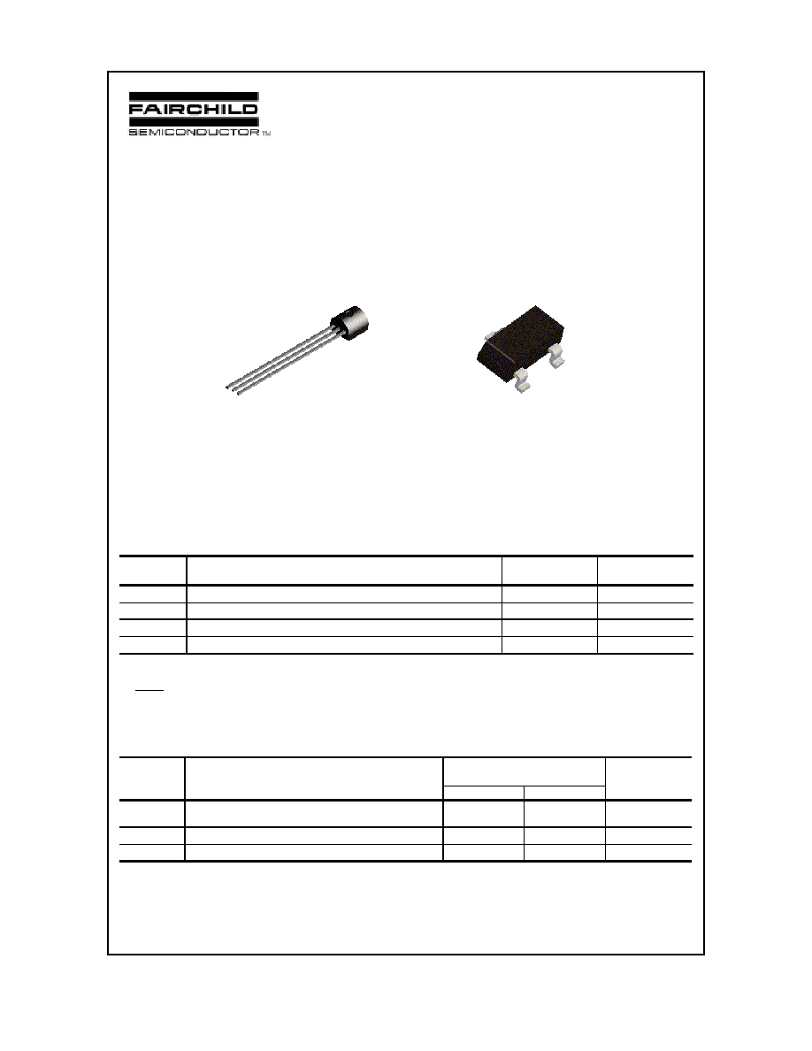
N-Channel Switch
This device is designed for low level analog switching, sample
and hold circuits and chopper stabalized amplifiers. Sourced
from Process 51. See J111 for characteristics.
Absolute Maximum Ratings*
TA = 25∞C unless otherwise noted
*
These ratings are limiting values above which the serviceability of any semiconductor device may be impaired.
NOTES:
1) These ratings are based on a maximum junction temperature of 150 degrees C.
2) These are steady state limits. The factory should be consulted on applications involving pulsed or low duty cycle operations
Thermal Characteristics
TA = 25∞C unless otherwise noted
Symbol
Parameter
Value
Units
V
DG
Drain-Gate Voltage
30
V
V
GS
Gate-Source Voltage
- 30
V
I
GF
Forward Gate Current
50
mA
T
J
,T
stg
Operating and Storage Junction Temperature Range
-55 to +150
∞
C
Symbol
Characteristic
Max
Units
PN4391
*MMBF4391
P
D
Total Device Dissipation
Derate above 25
∞
C
350
2.8
225
1.8
mW
mW/
∞
C
R
JC
Thermal Resistance, Junction to Case
125
∞
C/W
R
JA
Thermal Resistance, Junction to Ambient
357
556
∞
C/W
G
S
D
TO-92
SOT-23
Mark: 6J / 6K / 6G
G
S
D
*
Device mounted on FR-4 PCB 1.6" X 1.6" X 0.06."
Discrete POWER & Signal
Technologies
©
1997 Fairchild Semiconductor Corporation
PN4391 / PN4392 / PN4393 / MMBF4391 / MMBF4392 / MMBF4393
Electrical Characteristics
TA = 25∞C unless otherwise noted
Symbol
Parameter
Test Conditions
Min
Max
Units
OFF CHARACTERISTICS
ON CHARACTERISTICS
I
DSS
Zero-Gate Voltage Drain Current*
V
DS
= 20 V, V
GS
= 0
PN4391
PN4392
PN4393
50
25
5.0
150
75
30
mA
mA
mA
V
DS(
on
)
Drain-Source On Voltage
I
D
=
12 mA, V
GS
= 0
PN4391
I
D
=
6.0 mA, V
GS
= 0
PN4392
I
D
=
3.0 mA, V
GS
= 0
PN4393
0.4
0.4
0.4
V
V
V
r
DS(
on
)
Drain-Source On Resistance
I
D
=
1.0 mA, V
GS
= 0
PN4391
PN4392
PN4393
30
60
100
SMALL-SIGNAL CHARACTERISTICS
r
ds(on)
Drain-Source On Resistance
V
DS
= V
GS
= 0, f= 1.0 kHz PN4391
PN4392
PN4393
30
60
100
C
iss
Input Capacitance
V
DS
= 20, V
GS
= 0, f = 1.0 MHz
14
pF
C
rss
Reverse Transfer Capacitance
V
GS
= 12 V, f = 1.0 MHz
PN4391
V
GS
= 7.0 V, f = 1.0 MHz
PN4392
V
GS
= 5.0 V, f = 1.0 MHz
PN4393
3.5
3.5
3.5
pF
pF
pF
SWITCHING CHARACTERISTICS
t
r
Rise Time
I
D(
on
)
= 12 mA
PN4391
I
D(
on
)
= 6.0 mA PN4392
I
D(
on
)
= 3.0 mA
PN4393
5.0
5.0
5.0
ns
ns
ns
t
f
Fall Time
V
GS(
off)
= 12 V
PN4391
V
GS(
off)
= 6.0 V PN4392
V
GS(
off)
= 3.0 V
PN4393
15
20
30
ns
ns
ns
t
on
Turn-On Time
I
D(
on)
= 12 mA
PN4391
I
D(
on)
= 6.0 mA PN4392
I
D(
on)
= 3.0 mA
PN4393
15
15
15
ns
ns
ns
t
off
Turn-Off Time
V
GS(
off)
= 12 V
PN4391
V
GS(
off)
= 6.0 V PN4392
V
GS(
off)
= 3.0 V
PN4393
20
35
50
ns
ns
ns
*
Pulse Test: Pulse Width
300
µ
s, Duty Cycle
1.0%
V
(BR)GSS
Gate-Source Breakdown Voltage
I
G
= 1.0
µ
A, V
DS
= 0
- 30
V
I
GSS
Gate Reverse Current
V
GS
= 15 V, V
DS
= 0
V
GS
= 15 V, V
DS
= 0, T
A
= 150
∞
C
- 1.0
- 0.2
nA
µ
A
V
GS(off)
Gate-Source Cutoff Voltage
V
DS
= 20 V, I
D
= 1.0 nA
PN4391
PN4392
PN4393
- 4.0
- 2.0
- 0.5
- 10
- 5.0
- 3.0
V
V
V
V
GS(f)
Gate-Source Forward Voltage
I
G
= 1.0 mA, V
DS
= 0
1.0
V
I
D(off)
Drain Cutoff Leakage Current
V
DS
= 20 V, V
GS
= 12 V
PN4391
V
DS
= 20 V, V
GS
= 7.0 V PN4392
V
DS
= 20 V, V
GS
= 5.0 V PN4393
V
DS
= 20 V, V
GS
= 12 V, T
A
= 150
∞
C
PN4391
V
DS
= 20 V, V
GS
= 7.0 V,T
A
= 150
∞
C
PN4392
V
DS
= 20 V, V
GS
= 5.0 V,T
A
= 150
∞
C
PN4393
0.1
0.1
0.1
0.2
0.2
0.2
nA
nA
nA
µ
A
µ
A
µ
A
N-Channel Switch
(continued)