5
G
D
S
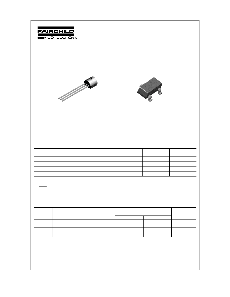
J201
J202
This device is designed primarily for low level audio and general
purpose applications with high impedance signal sources. Sourced
from Process 52.
Absolute Maximum Ratings*
TA = 25∞C unless otherwise noted
MMBFJ201
MMBFJ202
*
These ratings are limiting values above which the serviceability of any semiconductor device may be impaired.
NOTES:
1) These ratings are based on a maximum junction temperature of 150 degrees C.
2) These are steady state limits. The factory should be consulted on applications involving pulsed or low duty cycle operations
Thermal Characteristics
TA = 25∞C unless otherwise noted
N-Channel General Purpose Amplifier
Symbol
Parameter
Value
Units
V
DG
Drain-Gate Voltage
40
V
V
GS
Gate-Source Voltage
- 40
V
I
GF
Forward Gate Current
50
mA
T
J
,T
stg
Operating and Storage Junction Temperature Range
-55 to +150
∞
C
SOT-23
Mark: 62P / 62Q
G
S
D
TO-92
*
Device mounted on FR-4 PCB 1.6" X 1.6" X 0.06."
1997 Fairchild Semiconductor Corporation
NOTE: Source & Drain
are interchangeable
Symbol
Characteristic
Max
Units
J202-203
*MMBFJ202-203
P
D
Total Device Dissipation
Derate above 25
∞
C
625
5.0
350
2.8
mW
mW/
∞
C
R
JC
Thermal Resistance, Junction to Case
125
∞
C/W
R
JA
Thermal Resistance, Junction to Ambient
357
556
∞
C/W
J201 / J202 / MMBFJ201 / MMBFJ202
J201 / J202 / MMBFJ201 / MMBFJ202
N-Channel General Purpose Amplifier
(continued)
Electrical Characteristics
TA = 25∞C unless otherwise noted
OFF CHARACTERISTICS
Symbol
Parameter
Test Conditions
Min
Max
Units
V
(BR)GSS
Gate-Source Breakdown Voltage
I
G
= - 1.0
µ
A, V
DS
= 0
- 40
V
I
GSS
Gate Reverse Current
V
GS
= - 20 V, V
DS
= 0
-100
pA
V
GS(off)
Gate-Source Cutoff Voltage
V
DS
= 20 V, I
D
= 10 nA
201
202
- 0.3
- 0.8
- 1.5
- 4.0
V
V
ON CHARACTERISTICS
I
DSS
Zero-Gate Voltage Drain Current*
V
DS
= 20 V, I
GS
= 0
201
202
0.2
0.9
1.0
4.5
mA
mA
SMALL SIGNAL CHARACTERISTICS
y
fs
Forward Transfer Admittance
V
DS
= 20 V, f = 1.0 kHz
201
202
500
1000
µ
mhos
µ
mhos
*
Pulse Test: Pulse Width
300
µ
S
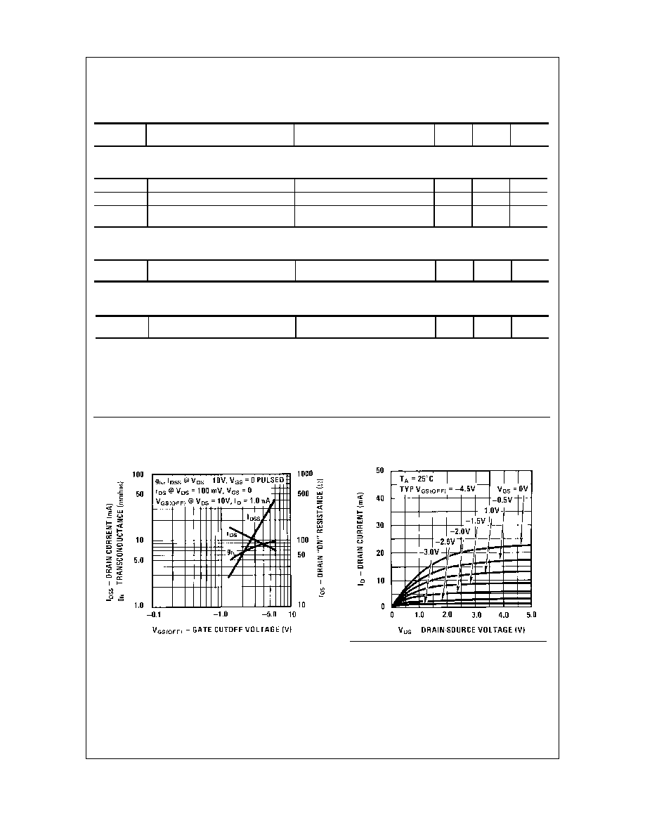
Typical Characteristics
Parameter Interactions
Common Drain-Source
5
Transfer Characteristics
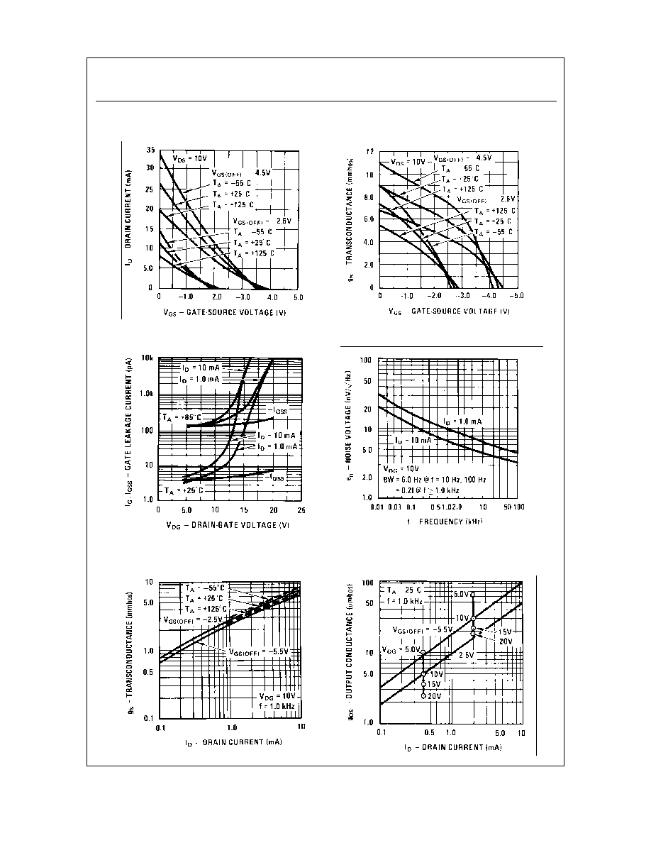
Typical Characteristics
(continued)
Output Conductance
vs. Drain Current
Leakage Current vs. Voltage
Noise Voltage vs. Frequency
Transfer Characteristics
Transconductance vs.
Drain Current
J201 / J202 / MMBFJ201 / MMBFJ202
N-Channel General Purpose Amplifier
(continued)
J201 / J202 / MMBFJ201 / MMBFJ202
N-Channel General Purpose Amplifier
(continued)
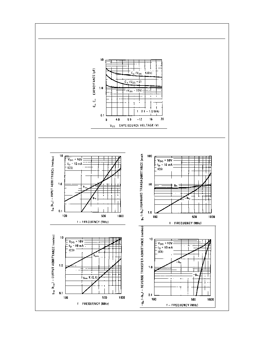
Typical Characteristics
(continued)
Common Source Characteristics
Input Admittance
Forward Transadmittance
Output Admittance
Reverse Transadmittance
Capacitance vs. Voltage
os)

5
Common Gate Characteristics
Input Admittance
Forward Transadmittance
Output Admittance
Reverse Transadmittance
J201 / J202 / MMBFJ201 / MMBFJ202
N-Channel General Purpose Amplifier
(continued)