 | –≠–ª–µ–∫—Ç—Ä–æ–Ω–Ω—ã–π –∫–æ–º–ø–æ–Ω–µ–Ω—Ç: MMBT5401 | –°–∫–∞—á–∞—Ç—å:  PDF PDF  ZIP ZIP |
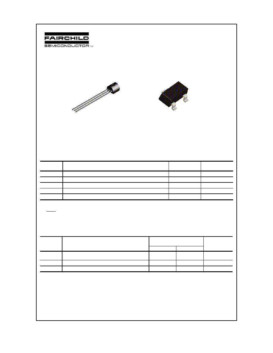
2N5401 / MMBT5401
PNP General Purpose Amplifier
This device is designed as a general purpose amplifier and switch
for applications requiring high voltages. Sourced from Process 74.
MMBT5401
2N5401
Absolute Maximum Ratings*
TA = 25∞C unless otherwise noted
*
These ratings are limiting values above which the serviceability of any semiconductor device may be impaired.
NOTES:
1) These ratings are based on a maximum junction temperature of 150 degrees C.
2) These are steady state limits. The factory should be consulted on applications involving pulsed or low duty cycle operations.
Symbol
Parameter
Value
Units
V
CEO
Collector-Emitter Voltage
150
V
V
CBO
Collector-Base Voltage
160
V
V
EBO
Emitter-Base Voltage
5.0
V
I
C
Collector Current - Continuous
200
mA
T
J
, T
stg
Operating and Storage Junction Temperature Range
-55 to +150
∞
C
Thermal Characteristics
TA = 25∞C unless otherwise noted
*
Device mounted on FR-4 PCB 1.6" X 1.6" X 0.06."
Symbol
Characteristic
Max
Units
2N5401
*MMBT5401
P
D
Total Device Dissipation
Derate above 25
∞
C
625
5.0
350
2.8
mW
mW/
∞
C
R
JC
Thermal Resistance, Junction to Case
83.3
∞
C/W
R
JA
Thermal Resistance, Junction to Ambient
200
357
∞
C/W
C
B
E
TO-92
C
B
E
SOT-23
Mark: 2L
Discrete POWER & Signal
Technologies
©
1997 Fairchild Semiconductor Corporation

2N5401 / MMBT5401
Electrical Characteristics
TA = 25∞C unless otherwise noted
OFF CHARACTERISTICS
V
(BR)CEO
Collector-Emitter Breakdown Voltage*
I
C
= 1.0 mA, I
B
= 0
150
V
V
(BR)CBO
Collector-Base Breakdown Voltage
I
C
= 100
µ
A, I
E
= 0
160
V
V
(BR)EBO
Emitter-Base Breakdown Voltage
I
E
= 10
µ
A, I
C
= 0
5.0
V
I
CBO
Collector Cutoff Current
V
CB
= 120 V, I
E
= 0
V
CB
= 120 V, I
E
= 0, T
A
= 100
∞
C
50
50
nA
µ
A
I
EBO
Emitter Cutoff Current
V
EB
= 3.0 V, I
C
= 0
50
nA
ON CHARACTERISTICS*
h
FE
DC Current Gain
I
C
= 1.0 mA, V
CE
= 5.0 V
I
C
= 10 mA, V
CE
= 5.0 V
I
C
= 50 mA, V
CE
= 5.0 V
50
60
50
240
V
CE(
sat
)
Collector-Emitter Saturation Voltage
I
C
= 10 mA, I
B
= 1.0 mA
I
C
= 50 mA, I
B
= 5.0 mA
0.2
0.5
V
V
V
BE(
sat
)
Base-Emitter Saturation Voltage
I
C
= 10 mA, I
B
= 1.0 mA
I
C
= 50 mA, I
B
= 5.0 mA
1.0
1.0
V
V
SMALL SIGNAL CHARACTERISTICS
f
T
Current Gain - Bandwidth Product
I
C
= 10 mA, V
CE
= 10 V,
f = 100 MHz
100
300
MHz
C
obo
Output Capacitance
V
CB
= 10 V, I
E
= 0,
f = 1.0 MHz
6.0
pF
NF
Noise Figure
I
C
= 250
µ
A, V
CE
= 5.0 V,
R
S
= 1.0 k
,
f = 10 Hz to 15.7 kHz
8.0
dB
*
Pulse Test: Pulse Width
300
µ
s, Duty Cycle
2.0%
Spice Model
PNP (Is=21.48f Xti=3 Eg=1.11 Vaf=100 Bf=132.1 Ne=1.375 Ise=21.48f Ikf=.1848 Xtb=1.5 Br=3.661 Nc=2
Isc=0 Ikr=0 Rc=1.6 Cjc=17.63p Mjc=.5312 Vjc=.75 Fc=.5 Cje=73.39p Mje=.3777 Vje=.75 Tr=1.476n Tf=641.9p
Itf=0 Vtf=0 Xtf=0 Rb=10)
Symbol
Parameter
Test Conditions
Min
Max
Units
PNP General Purpose Amplifier
(continued)

2N5401 / MMBT5401
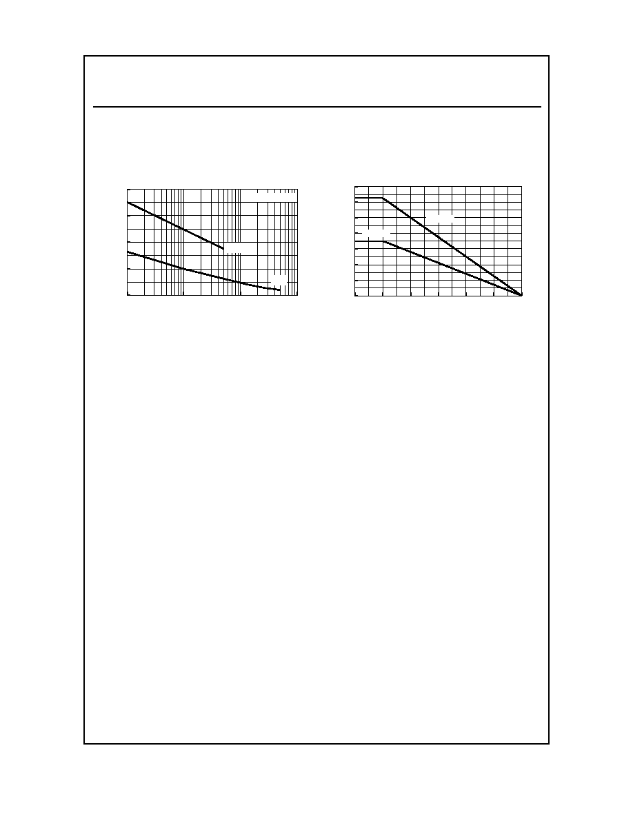
Typical Characteristics
PNP General Purpose Amplifier
(continued)
Collector-Emitter Saturation
Voltage vs Collector Current
P 74
0.1
1
10
100
0
0.1
0.2
0.3
0.4
I - COLLECTOR CURRENT (mA)
V
-
C
O
LLE
C
T
O
R
-
E
M
I
TTE
R
V
O
L
T
A
G
E
(
V
)
CE
S
A
T
C
= 10
125 ∫C
- 40 ∫C
25 ∞C
Base-Emitter Saturation
Voltage vs Collector Current
P
4
0.1
1
10
100
0.2
0.4
0.6
0.8
1
I - COLLECTOR CURRENT (mA)
V
-
B
A
SE-
EM
I
T
T
E
R
VO
L
T
A
G
E
(
V
)
B
ESA
T
C
= 10
125 ∫C
- 40 ∫C
25 ∞C
Base-Emitter ON Voltage vs
Collector Current
P 4
0.1
1
10
100
0.2
0.4
0.6
0.8
1
I - COLLECTOR CURRENT (mA)
V
-
B
A
SE-
EM
I
T
T
E
R
O
N
VO
L
T
A
G
E
(
V
)
B
E(O
N
)
125 ∫C
- 40 ∫C
25 ∞C
C
V = 5V
CE
Typical Pulsed Current Gain
vs Collector Current
0.0001
0.001
0.01
0.1
1
0
50
100
150
200
I - COLLECTOR CURRENT (A)
h
-
T
YPI
C
A
L
P
U
L
SED
C
U
R
R
EN
T
G
A
I
N
FE
- 40 ∫C
25 ∞C
C
V = 5V
CE
125 ∞C
Collector-Cutoff Current
vs Ambient Temperature
P 4
25
50
75
100
125
150
0.1
1
10
100
T - AMBIENT TEMPERATURE ( C)
I
-
C
O
L
L
E
CT
O
R
CU
RR
E
N
T
(n
A
)
A
V = 100V
CB
∫
CBO
Collector-Emitter Breakdown
Voltage with Resistance
Between Emitter-Base
0.1
1
10
100
1000
170
180
190
200
210
220
RESISTANCE (k )
B
V
-
B
R
E
A
K
D
O
W
N
VO
L
T
A
G
E
(
V
)
CE
R
2N5401 / MMBT5401
Typical Characteristics
(continued)
PNP General Purpose Amplifier
(continued)
Input and Output Capacitance
vs Reverse Voltage
0.1
1
10
100
0
20
40
60
80
V - REVERSE BIAS VOLTAGE(V)
CA
P
A
C
I
T
ANC
E
(
p
F
)
C
f = 1.0 MHz
R
C
cb
eb
Power Dissipation vs
Ambient Temperature
0
25
50
75
100
125
150
0
100
200
300
400
500
600
700
TEMPERATURE ( C)
P
-
P
O
W
E
R
D
I
SSI
P
A
T
I
O
N
(
m
W
)
D
o
TO-92
SOT-23