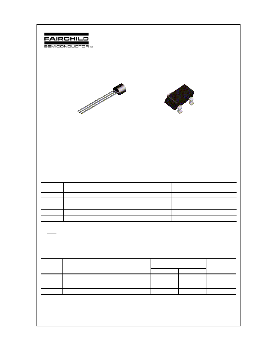
NPN RF Transistor
This device is designed for common-emitter low noise
amplifier and mixer applications with collector currents
in the 100
µ
A to 20 mA range to 300 MHz, and low
frequency drift common-base VHF oscillator applications
with high output levels for driving FET mixers. Sourced
from Process 47. See MPSH11 for characteristics.
MPSH24
MMBTH24
MPSH24 / MMBTH24
C
B
E
TO-92
C
B
E
SOT-23
Mark: 3A
Absolute Maximum Ratings*
TA = 25∞C unless otherwise noted
*
These ratings are limiting values above which the serviceability of any semiconductor device may be impaired.
NOTES:
1) These ratings are based on a maximum junction temperature of 150 degrees C.
2) These are steady state limits. The factory should be consulted on applications involving pulsed or low duty cycle operations
Thermal Characteristics
TA = 25∞C unless otherwise noted
Symbol
Parameter
Value
Units
V
CEO
Collector-Emitter Voltage
30
V
V
CBO
Collector-Base Voltage
40
V
V
EBO
Emitter-Base Voltage
4.0
V
I
C
Collector Current - Continuous
50
mA
T
J
, T
stg
Operating and Storage Junction Temperature Range
-55 to +150
∞
C
Symbol
Characteristic
Max
Units
MPSH24
*MMBTH24
P
D
Total Device Dissipation
Derate above 25
∞
C
625
5.0
225
1.8
mW
mW/
∞
C
R
JC
Thermal Resistance, Junction to Case
83.3
∞
C/W
R
JA
Thermal Resistance, Junction to Ambient
200
556
∞
C/W
*
Device mounted on FR-4 PCB 1.6" X 1.6" X 0.06."
Discrete POWER & Signal
Technologies
©
1997 Fairchild Semiconductor Corporation
Electrical Characteristics
TA = 25∞C unless otherwise noted
Symbol
Parameter
Test Conditions
Min
Max
Units
OFF CHARACTERISTICS
V
(BR)CEO
Collector-Emitter Sustaining Voltage*
I
C
= 1.0 mA, I
B
= 0
30
V
V
(BR)CBO
Collector-Base Breakdown Voltage
I
C
= 100
µ
A, I
E
= 0
40
V
V
(BR)EBO
Emitter-Base Breakdown Voltage
I
E
= 10
µ
A, I
C
= 0
4.0
V
I
CBO
Collector Cutoff Current
V
CB
= 15 V, I
E
= 0
50
nA
ON CHARACTERISTICS
h
FE
DC Current Gain
I
C
= 8.0 mA, V
CE
= 10 V
30
SMALL SIGNAL CHARACTERISTICS
f
T
Current Gain - Bandwidth Product
I
C
= 8.0 mA, V
CE
= 10 V,
f = 100 MHz
400
MHz
C
cb
Collector-Base Capacitance
V
CB
= 10 V, I
E
= 0, f = 1.0 MHz
0.36
pF
*
Pulse Test: Pulse Width
300
µ
s, Duty Cycle
2.0%
NPN RF Transistor
(continued)
MPSH24 / MMBTH24