 | ÐлекÑÑоннÑй компоненÑ: NC7NZU04 | СкаÑаÑÑ:  PDF PDF  ZIP ZIP |
Äîêóìåíòàöèÿ è îïèñàíèÿ www.docs.chipfind.ru
© 2003 Fairchild Semiconductor Corporation
DS500490
www.fairchildsemi.com
July 2001
Revised April 2003
NC7NZU04 T
i
nyLogi
c
UHS Unbuff
e
red In
vert
e
r
NC7NZU04
TinyLogic
UHS Unbuffered Inverter
General Description
The NC7NZU04 is a triple unbuffered inverter from
Fairchild's Ultra High Speed Series of TinyLogic
. The
special purpose unbuffered circuit design is primarily
intended for crystal oscillator or analog applications. The
device is fabricated with advanced CMOS technology to
achieve ultra high speed with high output drive while main-
taining low static power dissipation over a very broad V
CC
operating range. The device is specified to operate over
the 1.65V to 5.5V V
CC
range.
Features
s
Space saving US8 surface mount package
s
MicroPak
leadless package
s
Unbuffered for crystal oscillator and analog applications
s
Balanced Output Drive;
±
8 mA at 4.5V V
CC
s
Broad V
CC
Operating Range: 1.65V to 5.5V
s
Low Quiescent Power;
I
CC
<
1
µ
A, V
CC
=
5.5V, T
A
=
25
°
C
Ordering Code:
TinyLogic
is a registered trademark of Fairchild Semiconductor Corporation.
MicroPak
is a trademark of Fairchild Semiconductor Corporation.
Product
Package Description
Supplied As
Order
Package
Code
Number
Number
Top Mark
NC7NZU04K8X
MAB08A
7NZU4
8-Lead US8, JEDEC MO-187, Variation CA 3.1mm Wide 3k Units on Tape and Reel
NC7NZU04L8X
(Preliminary)
MAC08A
U6
8-Lead MicroPak, 1.6 mm Wide
5k Units on Tape and Reel
www.fairchildsemi.com
2
NC
7
N
ZU04
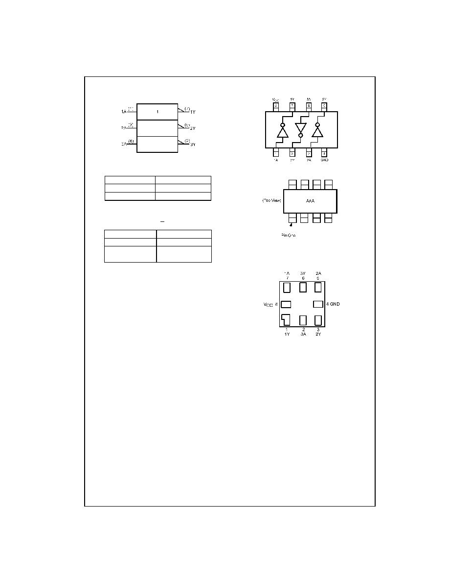
Logic Symbol
IEEE/IEC
Pin Descriptions
Function Table
H
=
HIGH Logic Level
L
=
LOW Logic Level
Connection Diagrams
(Top View)
AAA represents Product Code Top Mark - see ordering code
Note: Orientation of Top Mark determines Pin One location. Read the Top
Product Code Mark left to right, Pin One is the lower left pin (see diagram).
Pad Assignment for MicroPak
(Top Thru View)
Pin Names
Description
A
Input
Y
Output
Y
=
A
Input
Output
A
Y
L
H
H
L
3
www.fairchildsemi.com
NC7NZU04
Absolute Maximum Ratings
(Note 1)
Recommended Operating
Conditions
(Note 2)
Note 1: Absolute maximum ratings are DC values beyond which the device
may be damaged or have its useful life impaired. The datasheet specifica-
tions should be met, without exception, to ensure that the system design is
reliable over its power supply, temperature, and output/input loading vari-
ables. Fairchild does not recommend operation outside datasheet specifi-
cations.
Note 2: Unused inputs must be held HIGH or LOW. They may not float.
DC Electrical Characteristics
Supply Voltage (V
CC
)
-
0.5V to
+
7V
DC Input Voltage (V
IN
)
-
0.5V to
+
7V
DC Output Voltage (V
OUT
)
-
0.5V to
+
7V
DC Input Diode Current (I
IK
)
@ V
IN
<
-
0.5V
-
50 mA
@ V
IN
>
V
CC
+
0.5V
+
20 mA
DC Output Diode Current (I
OK
)
@ V
OUT
<
-
0.5V
-
50 mA
@ V
OUT
>
0.5V, V
CC
=
GND
+
50 mA
DC Output Current (I
OUT
)
±
50 mA
DC V
CC
/GND Current (I
CC
/I
GND
)
±
100 mA
Storage Temperature (T
STG
)
-
65
°
C to
+
150
°
C
Junction Temperature under Bias (T
J
)
150
°
C
Junction Lead Temperature (T
L
);
(Soldering, 10 seconds)
260
°
C
Power Dissipation (P
D
) @
+
85
°
C
250 mW
Supply Voltage Operating (V
CC
)
1.65V to 5.5V
Supply Voltage Data Retention (V
CC
)
1.5V to 5.5V
Input Voltage (V
IN
)
0V to 5.5V
Output Voltage (V
OUT
)
0V to V
CC
Operating Temperature (T
A
)
-
40
°
C to
+
85
°
C
Thermal Resistance (
JA
)
250
°
C/W
Symbol
Parameter
V
CC
T
A
=
+
25
°
C
T
A
=
-
40
°
C to
+
85
°
C
Units
Conditions
(V)
Min
Typ
Max
Min
Max
V
IH
HIGH Level Input Voltage
1.65 to 2.7 0.85 V
CC
0.85 V
CC
V
3.0 to 5.5
0.8 V
CC
0.8 V
CC
V
IL
LOW Level Input Voltage
1.65 to 2.7
0.15 V
CC
0.15 V
CC
V
3.0 to 5.5
0.2 V
CC
0.2 V
CC
V
OH
HIGH Level Output Voltage
1.65
1.55
1.65
1.55
V
V
IN
=
V
IL
I
OH
=
-
100
µ
A
2.3
2.1
2.3
2.1
3.0
2.7
3.0
2.7
4.5
4.0
4.4
4.0
1.65
1.29
1.52
1.29
I
OH
=
-
2 mA
2.3
1.9
2.14
1.9
V
IN
=
GND
I
OH
=
-
2 mA
3.0
2.4
2.75
2.4
I
OH
=
-
4 mA
3.0
2.3
2.61
2.3
I
OH
=
-
6 mA
4.5
3.8
4.13
3.8
I
OH
=
-
8 mA
V
OL
LOW Level Output Voltage
1.65
0.0
0.2
0.2
V
V
IN
=
V
IH
I
OL
=
100
µ
A
2.3
0.0
0.2
0.2
3.0
0.0
0.3
0.3
4.5
0.0
0.5
0.5
1.65
0.08
0.24
0.24
I
OL
=
2
mA
2.3
0.10
0.3
0.3
V
IN
=
V
CC
I
OL
=
2
mA
3.0
0.17
0.4
0.4
I
OL
=
4 mA
3.0
0.25
0.55
0.55
I
OL
=
6 mA
4.5
0.26
0.55
0.55
I
OL
=
8 mA
I
IN
Input Leakage Current
0 to 5.5
±
0.1
±
1.0
µ
A
V
IN
=
5.5V, GND
I
CC
Quiescent Supply Current
1.65 to 5.5
1
10
µ
A
V
IN
=
5.5V, GND
I
CCPEAK
Peak Supply Current in
1.8
1
mA
V
OUT
=
Open
Analog Operation
2.5
2
V
IN
=
Adjust for
3.3
5
Peak I
CC
Current
5.0
15
www.fairchildsemi.com
4
NC
7
N
ZU04
AC Electrical Characteristics
Note 3: C
PD
is defined as the value of the internal equivalent capacitance which is derived from dynamic operating current consumption (I
CCD
) at no output
loading and operating at 50% duty cycle. (See Figure 2.) C
PD
is related to I
CCD
dynamic operating current by the expression:
I
CCD
=
(C
PD
)(V
CC
)(f
IN
)
+
(I
CC
static).
Dynamic Switching Characteristics
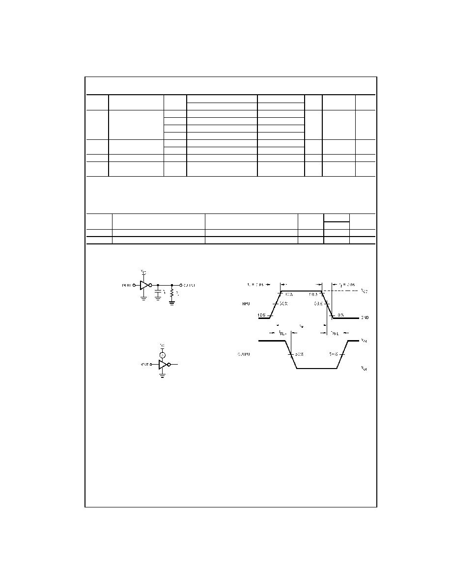
AC Loading and Waveforms
C
L
includes load and stray capacitance
Input PRR
=
1.0 MHz; t
W
=
500 ns
FIGURE 1. AC Test Circuit
Application Note: When operating the NC7NZU04's unbuffered output
stage in its linear range, as in oscillator applications, care must be taken to
observe maximum power rating for the device and package. The high drive
nature of the design of the output stage will result in substantial simulta-
neous conduction currents when the stage is in the linear region. See the
I
CCPEAK
specification in the DC Electrical Characteristics table.
Input
=
AC Waveform; t
r
=
t
f
=
1.8 ns;
PRR
=
variable; Duty Cycle
=
50%
FIGURE 2. I
CCD
Test Circuit
FIGURE 3. AC Waveforms
Symbol
Parameter
V
CC
T
A
=
+
25
°
C
T
A
=
-
40
°
C to
+
85
°
C
Units
Conditions
Figure
Number
(V)
Min
Typ
Max
Min
Max
t
PLH
,
Propagation Delay
1.8
±
0.05
1.0
8.5
1.0
9.0
ns
Figures
1, 3
t
PHL
2.5
±
0.2
0.8
6.2
0.8
6.5
C
L
=
15 pF,
3.3
±
0.3
0.5
4.5
0.5
4.8
R
L
=
1 M
5.0
±
0.5
0.5
3.9
0.5
4.1
t
PLH
,
Propagation Delay
3.3
±
0.3
1.0
6.0
1.0
6.5
ns
C
L
=
50 pF,
Figures
1, 3
t
PHL
5.0
±
0.5
0.8
5.0
0.8
5.5
R
L
=
500
C
IN
Input Capacitance
0
2.5
pF
C
PD
Power Dissipation
3.3
9
pF
(Note 3)
Figure 2
Capacitance
5.0
11
Symbol
Parameter
Conditions
V
CC
T
A
=
25
°
C
Unit
(V)
Typical
V
OLP
Quiet Output Dynamic Peak V
OL
C
L
=
50pF, V
IH
=
5.0V, V
IL
=
0V
5.0
0.8
V
V
OLV
Quiet Output Dynamic Valley V
OL
C
L
=
50pF, V
IH
=
5.0V, V
IL
=
0V
5.0
-
0.8
V
5
www.fairchildsemi.com
NC7NZU04
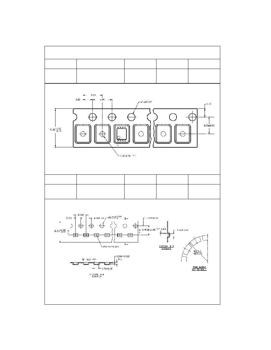
Tape and Reel Specification
TAPE FORMAT for US8
TAPE DIMENSIONS inches (millimeters)
TAPE FORMAT for MicroPak
TAPE DIMENSIONS inches (millimeters)
Package
Tape
Number
Cavity
Cover Tape
Designator
Section
Cavities
Status
Status
Leader (Start End)
125 (typ)
Empty
Sealed
K8X
Carrier
3000
Filled
Sealed
Trailer (Hub End)
75 (typ)
Empty
Sealed
Package
Tape
Number
Cavity
Cover Tape
Designator
Section
Cavities
Status
Status
Leader (Start End)
125 (typ)
Empty
Sealed
L8X
Carrier
3000
Filled
Sealed
Trailer (Hub End)
75 (typ)
Empty
Sealed
www.fairchildsemi.com
6
NC
7
N
ZU04
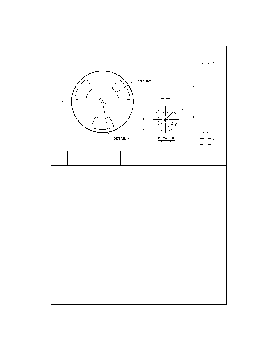
Tape and Reel Specification
(Continued)
REEL DIMENSIONS inches (millimeters)
Tape Size
A
B
C
D
N
W1
W2
W3
8 mm
7.0
0.059
0.512
0.795
2.165
0.331
+
0.059/
-
0.000
0.567
W1
+
0.078/
-
0.039
(177.8)
(1.50)
(13.00)
(20.20)
(55.00)
(8.40
+
1.5/
-
0.00)
(14.40)
(W1
+
2.00/
-
1.00)
7
www.fairchildsemi.com
NC7NZU04
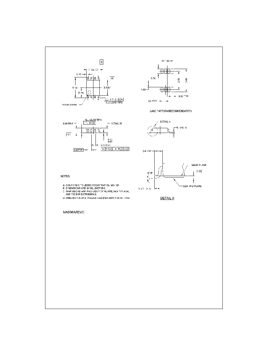
Physical Dimensions
inches (millimeters) unless otherwise noted
8-Lead US8, JEDEC MO-187, Variation CA 3.1mm Wide
Package Number MAB08A
www.fairchildsemi.com
8
NC7NZU04 T
i
nyLogi
c
UHS Unbuf
fer
ed I
nver
ter
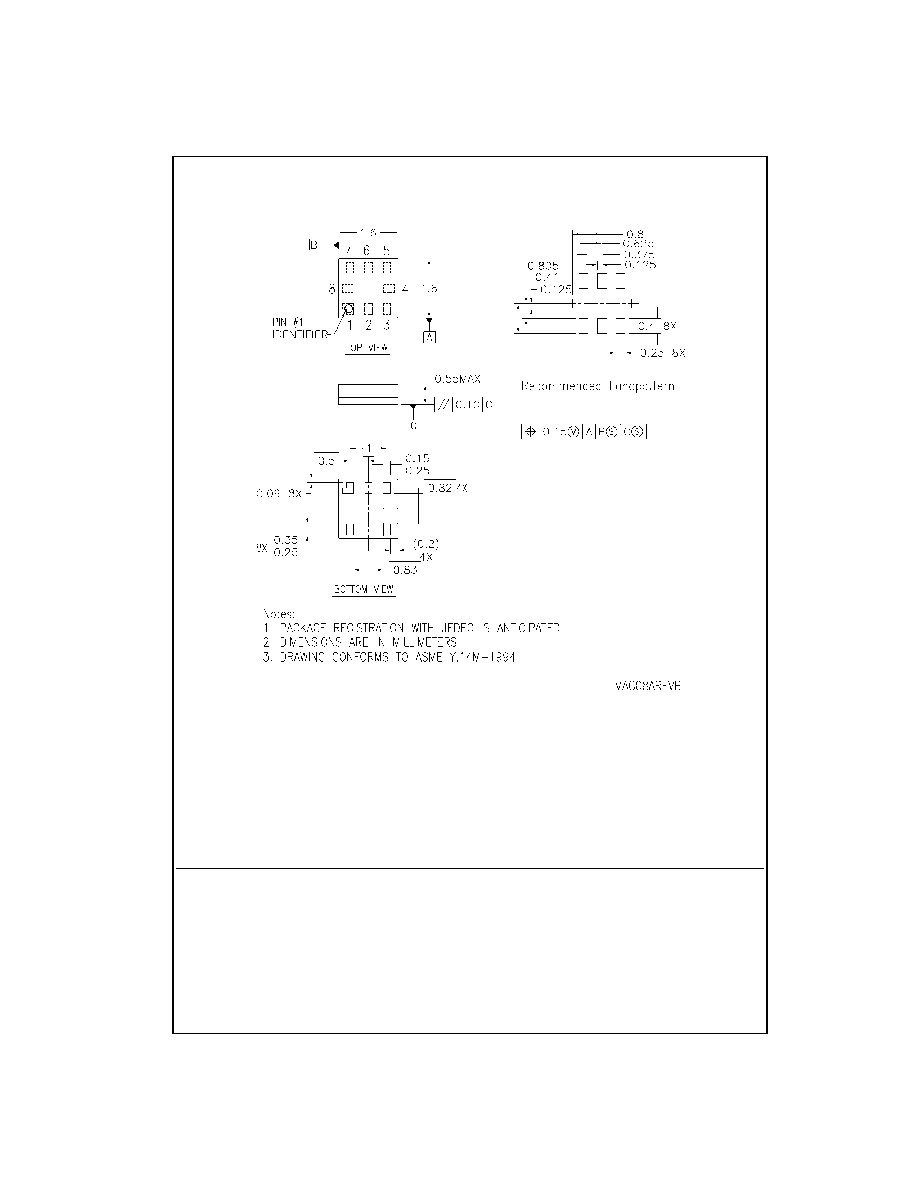
Physical Dimensions
inches (millimeters) unless otherwise noted (Continued)
8-Lead MicroPak, 1.6 mm Wide
Package Number MAC08A
(Preliminary)
Fairchild does not assume any responsibility for use of any circuitry described, no circuit patent licenses are implied and
Fairchild reserves the right at any time without notice to change said circuitry and specifications.
LIFE SUPPORT POLICY
FAIRCHILD'S PRODUCTS ARE NOT AUTHORIZED FOR USE AS CRITICAL COMPONENTS IN LIFE SUPPORT
DEVICES OR SYSTEMS WITHOUT THE EXPRESS WRITTEN APPROVAL OF THE PRESIDENT OF FAIRCHILD
SEMICONDUCTOR CORPORATION. As used herein:
1. Life support devices or systems are devices or systems
which, (a) are intended for surgical implant into the
body, or (b) support or sustain life, and (c) whose failure
to perform when properly used in accordance with
instructions for use provided in the labeling, can be rea-
sonably expected to result in a significant injury to the
user.
2. A critical component in any component of a life support
device or system whose failure to perform can be rea-
sonably expected to cause the failure of the life support
device or system, or to affect its safety or effectiveness.
www.fairchildsemi.com