 | –≠–ª–µ–∫—Ç—Ä–æ–Ω–Ω—ã–π –∫–æ–º–ø–æ–Ω–µ–Ω—Ç: NC7SV57 | –°–∫–∞—á–∞—Ç—å:  PDF PDF  ZIP ZIP |
© 2003 Fairchild Semiconductor Corporation
DS500671
www.fairchildsemi.com
June 2002
Revised January 2003
NC7SV57 ∑
NC7SV58 T
i
nyLogi
c
ULP-
A Uni
versal
C
o
nfi
gurabl
e
2
-
I
nput
Logi
c Gat
e
s
NC7SV57 ∑ NC7SV58
TinyLogic
ULP-A Universal Configurable
2-Input Logic Gates
General Description
The NC7SV57 and NC7SV58 are universal configurable
2-input logic gates from Fairchild's Ultra Low Power
(ULP-A) Series of TinyLogic
. ULP-A is ideal for applica-
tions that require extreme high speed, high drive and low
power. This product is designed for a wide low voltage
operating range (0.9V to 3.6V V
CC
) and applications that
require more drive and speed than the TinyLogic ULP
series, but still offer best in class low power operation.
Each device is capable of being configured for 1 of 5
unique 2-input logic functions. Any possible 2-input combi-
natorial logic function can be implemented as shown in the
Function Selection Table. Device functionality is selected
by how the device is wired at the board level. Figure 1
through Figure 10 illustrate how to connect the NC7SV57
and NC7SV58 respectively for the desired logic function.
All inputs have been implemented with hysteresis.
The NC7SV57 and NC7SV58 are uniquely designed for
optimized power and speed, and are fabricated with an
advanced CMOS technology to achieve high-speed opera-
tion while maintaining low CMOS power dissipation.
Features
s
0.9V to 3.6V V
CC
supply operation
s
3.6V overvoltage tolerant I/O's at V
CC
from 0.9V to 3.6V
s
Extremely High Speed t
PD
2.5 ns typ for 2.7V to 3.6V V
CC
3.1 ns typ for 2.3V to 2.7V V
CC
4.0 ns typ for 1.65V to 1.95V V
CC
6.0 ns typ for 1.4V to 1.6V V
CC
8.0 ns typ for 1.1V to 1.3V V
CC
23.0 ns typ for 0.9V V
CC
s
Power-Off high impedance inputs and outputs
s
High Static Drive (I
OH
/I
OL
)
±
24 mA @ 3.00V V
CC
±
18 mA @ 2.30V V
CC
±
6 mA
@ 1.65V V
CC
±
4 mA
@ 1.4V V
CC
±
2 mA
@ 1.1V V
CC
±
0.1 mA @ 0.9V V
CC
s
Uses patented Quiet Series
noise/EMI reduction
circuitry
s
Ultra small MicroPak
leadfree package
s
Ultra low Dynamic Power
Ordering Code:
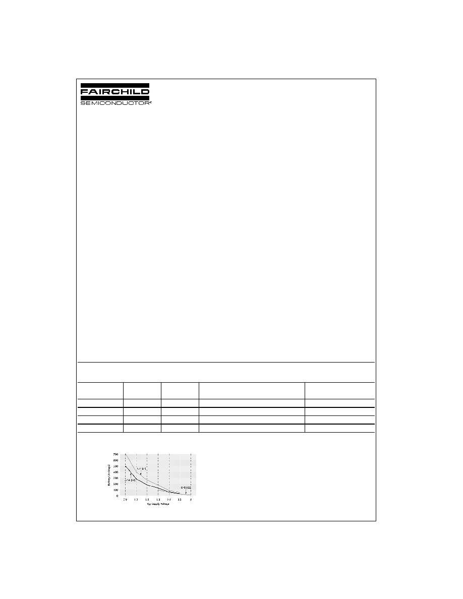
Battery Life vs. V
CC
Supply Voltage
TinyLogic ULP and ULP-A with up to 50% less power consumption can
extend your battery life significantly.
Battery Life
=
(V
battery
*I
battery
*.9)/(P
device
)/24hrs/day
Where, P
device
=
(I
CC
* V
CC
)
+
(C
PD
+
C
L
) * V
CC
2
* f
Assumes ideal 3.6V Lithium Ion battery with current rating of 900mAH and
derated 90% and device frequency at 10MHz, with C
L
=
15 pF load
TinyLogic
, MicroPak
, and Quiet Series
are trademarks of Fairchild Semiconductor Corporation.
Order Number
Package Product
Code
Package Description
Supplied As
Number
Top Mark
NC7SV57P6X
MAA06A
V57
6-Lead SC70, EIAJ SC88, 1.25mm Wide
3k Units on Tape and Reel
NC7SV57L6X
MAC06A
H3
6-Lead MicroPak, 1.0mm Wide
5k Units on Tape and Reel
NC7SV58P6X
MAA06A
V58
6-Lead SC70, EIAJ SC88, 1.25mm Wide
3k Units on Tape and Reel
NC7SV58L6X
MAC06A
H4
6-Lead MicroPak, 1.0mm Wide
5k Units on Tape and Reel
www.fairchildsemi.com
2
NC
7
S
V57
∑
NC
7
S
V58
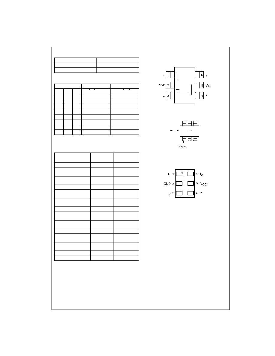
Pin Descriptions
Function Table
H
=
HIGH Logic Level
L
=
LOW Logic Level
Function Selection Table
Connection Diagrams
Pin Assignments for SC70
(Top View)
Pin One Orientation Diagram
AAA represents Product Code Top Mark - see ordering code
Note: Orientation of Top Mark determines Pin One location. Read the top
product code mark left to right, Pin One is the lower left pin (see diagram).
Pad Assignments for MicroPak
(Top Thru View)
Pin Name
Description
I
0
, I
1
, I
2
Data Inputs
Y
Output
Inputs
NC7SV57
NC7SV58
I
2
I
1
I
0
Y
=
(I
0
)∑(I
2
)
+
(I
1
)∑(I
2
) Y
=
(I
0
)∑(I
2
)
+
(I
1
)∑(I
2
)
L
L
L
H
L
L
L
H
L
H
L
H
L
H
L
L
H
H
L
H
H
L
L
L
H
H
L
H
L
H
H
H
L
H
L
H
H
H
H
L
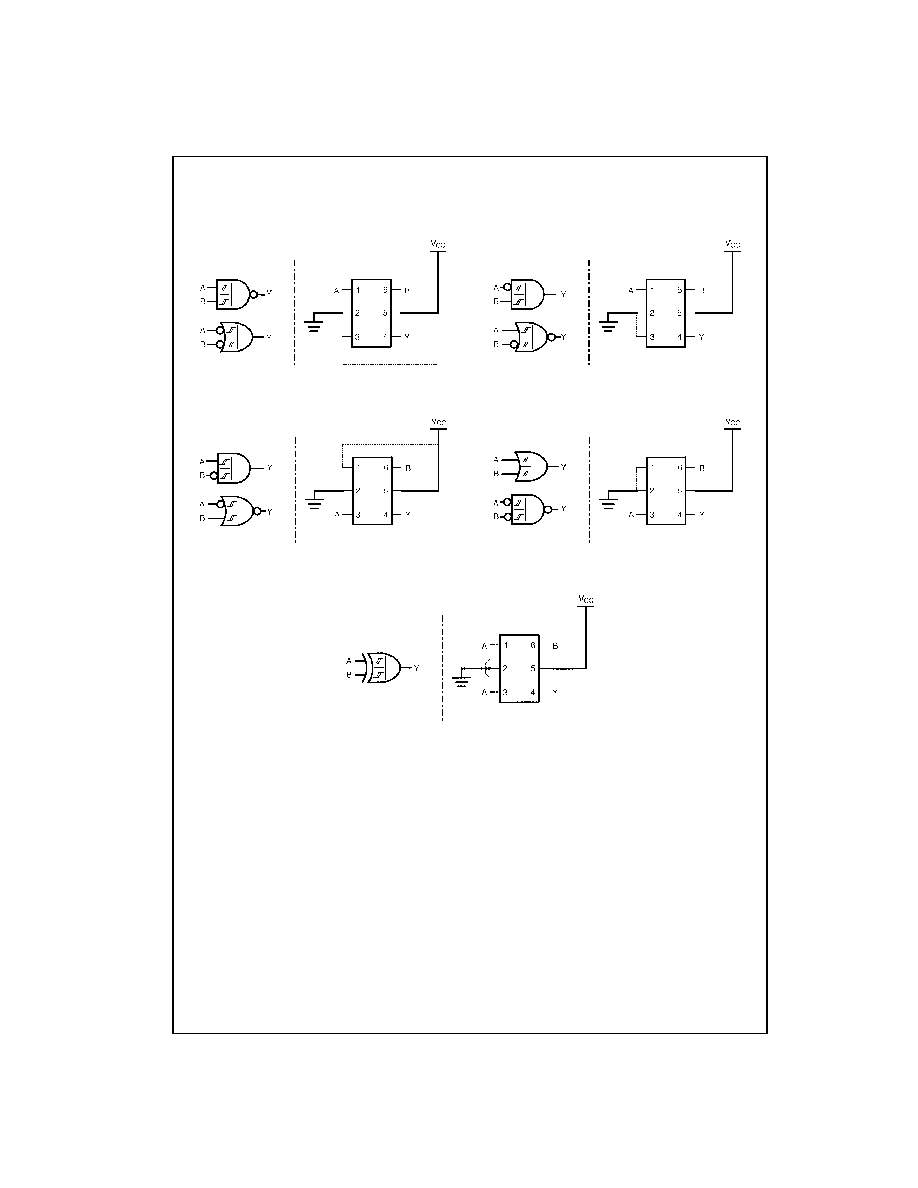
2-Input Logic Function
Device Connection
Selection
Configuration
2-Input AND
NC7SV57
Figure 1
2-Input AND
with inverted input
NC7SV58
Figures 7, 8
2-Input AND
with both inputs inverted
NC7SV57
Figure 4
2-Input NAND
NC7SV58
Figure 6
2-Input NAND
with inverted input
NC7SV57
Figures 2, 3
2-Input NAND
with both inputs inverted
NC7SV58
Figure 9
2-Input OR
NC7SV58
Figure 9
2-Input OR
with inverted input
NC7SV57
Figures 2, 3
2-Input OR
with both inputs inverted
NC7SV58
Figure 6
2-Input NOR
NC7SV57
Figure 4
2-Input NOR
with inverted input
NC7SV58
Figures 7, 8
2-Input NOR
with both inputs inverted
NC7SV57
Figure 1
2-Input XOR
NC7SV58
Figure 10
2-Input XNOR
NC7SV57
Figure 5

3
www.fairchildsemi.com
NC7SV57
∑
NC7SV58
Logic Configurations NC7SV57
Figure 1 through Figure 5 show the logical functions that can be implemented using the NC7SV57. The diagrams show the
DeMorgan's equivalent logic duals for a given 2-input function. Next to the logical implementation is the board level physical
implementation of how the pins of the function should be connected.
FIGURE 1. 2-Input AND Gate
FIGURE 2. 2-Input NAND with Inverted A Input
FIGURE 3. 2-Input NAND with Inverted B Input
FIGURE 4. 2-Input NOR Gate
FIGURE 5. 2-Input XNOR Gate
www.fairchildsemi.com
4
NC
7
S
V57
∑
NC
7
S
V58
Logic Configurations NC7SV58
Figure 6 through Figure 10 show the logical functions that can be implemented using the NC7SV58. The diagrams show
the DeMorgan's equivalent logic duals for a given 2-input function. Next to the logical implementation is the board level
physical implementation of how the pins of the function should be connected.
FIGURE 6. 2-Input NAND Gate
FIGURE 7. 2-Input AND with Inverted A Input
FIGURE 8. 2-Input AND with Inverted B Input
FIGURE 9. 2-Input OR Gate
FIGURE 10. 2-Input XOR Gate
5
www.fairchildsemi.com
NC7SV57
∑
NC7SV58
Absolute Maximum Ratings
(Note 1)
Recommended Operating
Conditions
(Note 3)
Note 1: Absolute Maximum Ratings: are those values beyond which the
safety of the device cannot be guaranteed. The device should not be oper-
ated at these limits. The parametric values defined in the Electrical Charac-
teristics tables are not guaranteed at the absolute maximum ratings. The
"Recommended Operating Conditions" table will define the conditions for
actual device operation.
Note 2: I
O
Absolute Maximum Rating must be observed.
Note 3: Unused inputs must be held HIGH or LOW. They may not float.
DC Electrical Characteristics
Supply Voltage (V
CC
)
-
0.5V to
+
4.6V
DC Input Voltage (V
IN
)
-
0.5V to
+
4.6V
DC Output Voltage (V
OUT
)
HIGH or LOW State (Note 2)
-
0.5V to V
CC
+
0.5V
V
CC
=
0V
-
0.5V to
+
4.6V
DC Input Diode Current (I
IK
) V
IN
<
0V
±
50 mA
DC Output Diode Current (I
OK
)
V
OUT
<
0V
-
50 mA
V
OUT
>
V
CC
+
50 mA
DC Output Source/Sink Current (I
OH
/I
OL
)
±
50 mA
DC V
CC
or Ground Current per
Supply Pin (I
CC
or Ground)
±
50 mA
Storage Temperature Range (T
STG
)
-
65
∞
C to
+
150
∞
C
Supply Voltage
0.9V to 3.6V
Input Voltage (V
IN
)
0V to 3.6V
Output Voltage (V
OUT
)
V
CC
=
0.0V
0V to 3.6V
HIGH or LOW State
0V to V
CC
Output Current in I
OH
/I
OL
V
CC
=
3.0V to 3.6V
±
24 mA
V
CC
=
2.3V to 2.7V
±
18 mA
V
CC
=
1.65V to 1.95V
±
6 mA
V
CC
=
1.4V to 1.6V
±
4 mA
V
CC
=
1.1V to 1.3V
±
2 mA
V
CC
=
0.9V
±
0.1 mA
Free Air Operating Temperature (T
A
)
-
40
∞
C to
+
85
∞
C
Minimum Input Edge Rate (
t/
V)
V
IN
=
0.8V to 2.0V, V
CC
=
3.0V
10 ns/V
Symbol
Parameter
V
CC
T
A
=
+
25
∞
C
T
A
=
-
40
∞
C to
+
85
∞
C
Units
Conditions
(V)
Min
Max
Min
Max
V
P
Positive Threshold Voltage
0.90
0.3
0.7
0.3
0.7
V
1.10
0.4
1.0
0.4
1.0
1.40
0.5
1.4
0.5
1.4
1.65
0.7
1.5
0.7
1.5
2.30
1.0
1.8
1.0
1.8
2.70
1.3
2.2
1.3
2.2
V
N
Negative Threshold Voltage
0.90
0.10
0.6
0.1
0.6
V
1.10
0.15
0.7
0.15
0.7
1.40
0.2
0.8
0.2
0.8
1.65
0.25
0.9
0.25
0.9
2.30
0.4
1.15
0.4
1.15
2.70
0.6
1.5
0.6
1.5
V
H
Hysteresis Voltage
0.90
0.07
0.5
0.07
0.5
V
1.10
0.08
0.6
0.08
0.6
1.40
0.1
0.8
0.1
0.8
1.65
0.15
1.0
0.15
1.0
2.30
0.25
1.1
0.25
1.1
2.70
0.40
1.2
0.40
1.2

www.fairchildsemi.com
6
NC
7
S
V57
∑
NC
7
S
V58
DC Electrical Characteristics
(Continued)
AC Electrical Characteristics
Symbol
Parameter
V
CC
T
A
=
+
25
∞
C
T
A
=
-
40
∞
C to
+
85
∞
C
Units
Conditions
(V)
Min
Max
Min
Max
V
OH
HIGH Level
0.90
V
CC
-
0.1
V
CC
-
0.1
V
I
OH
=
-
100
µ
A
Output Voltage
1.10
V
CC
1.30
V
CC
-
0.1
V
CC
-
0.1
1.40
V
CC
1.60
V
CC
-
0.2
V
CC
-
0.2
1.65
V
CC
1.95
V
CC
-
0.2
V
CC
-
0.2
2.30
V
CC
<
2.70
V
CC
-
0.2
V
CC
-
0.2
2.70
V
CC
3.60
V
CC
-
0.2
V
CC
-
0.2
1.10
V
CC
1.30
0.75 x V
CC
0.75 x V
CC
I
OH
=
-
2 mA
1.40
V
CC
1.60
0.75 x V
CC
0.75 x V
CC
I
OH
=
-
4 mA
1.65
V
CC
1.95
1.25
1.25
I
OH
=
-
6 mA
2.30
V
CC
<
2.70
2.0
2.0
2.30
V
CC
<
2.70
1.8
1.8
I
OH
=
-
12 mA
2.70
V
CC
3.60
2.2
2.2
2.30
V
CC
<
2.70
1.7
1.7
I
OH
=
-
18 mA
2.70
V
CC
3.60
2.4
2.4
2.70
V
CC
3.60
2.2
2.2
I
OH
=
-
24 mA
V
OL
LOW Level
0.90
0.1
0.1
V
I
OL
=
100
µ
A
Output Voltage
1.10
V
CC
1.30
0.1
0.1
1.40
V
CC
1.60
0.2
0.2
1.65
V
CC
1.95
0.2
0.2
2.30
V
CC
<
2.70
0.2
0.2
2.70
V
CC
3.60
0.2
0.2
1.10
V
CC
1.30
0.25 x V
CC
0.25 x V
CC
I
OL
=
2 mA
1.40
V
CC
1.60
0.25 x V
CC
0.25 x V
CC
I
OL
=
4 mA
1.65
V
CC
1.95
0.3
0.3
I
OL
=
6 mA
2.30
V
CC
<
2.70
0.4
0.4
I
OL
=
12 mA
2.70
V
CC
3.60
0.4
0.4
2.30
V
CC
<
2.70
0.6
0.6
I
OL
=
18 mA
2.70
V
CC
3.60
0.4
0.4
2.70
V
CC
3.60
0.55
0.55
I
OL
=
24 mA
I
IN
Input Leakage Current
0.90 to 3.60
±
0.1
±
0.9
µ
A
0
V
I
3.6V
I
OFF
Power Off Leakage Current
0
1
5
µ
A
0
(V
I
, V
O
)
3.6V
I
CC
Quiescent Supply Current
0.90 to 3.60
0.9
5
µ
A
V
I
=
V
CC
or GND
0.90 to 3.60
±
5
V
CC
V
I
3.6V
Symbol
Parameter
V
CC
T
A
=
+
25
∞
C
T
A
=
-
40
∞
C to
+
85
∞
C
Units
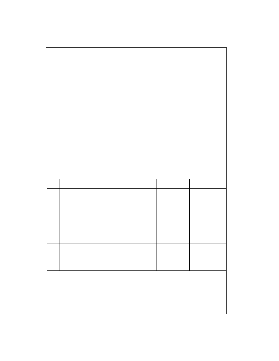
Conditions
Figure
Number
(V)
Min
Typ
Max
Min
Max
t
PHL
Propagation Delay
0.90
15
ns
C
L
=
15 pF, R
L
=
1 M
Figures
11, 12
t
PLH
1.10
V
CC
1.30
4.0
8
16.5
3.3
31.0
C
L
=
15 pF, R
L
=
2 k
1.40
V
CC
1.60
2.0
6
10.0
2.0
12.0
1.65
V
CC
1.95
2.0
4
9.1
1.9
10.0
C
L
=
30 pF
2.30
V
CC
<
2.70
1.5
3.1
6.2
1.4
6.7
R
L
=
500
2.70
V
CC
3.60
1.2
2.5
5.4
1.2
6.1
C
IN
Input Capacitance
0
8.0
pF
C
OUT
Output Capacitance
0
12.0
pF
C
PD
Power Dissipation
0.90 to 3.60
10
pF
V
I
=
0V or V
CC
Capacitance
f
=
10 MHz

7
www.fairchildsemi.com
NC7SV57
∑
NC7SV58
AC Loading and Waveforms
FIGURE 11. AC Test Circuit
FIGURE 12. AC Waveforms
Symbol
V
CC
3.3V
±
0.3V
2.5V
±
0.2V
1.8V
±
0.15V
1.5V
±
0.10V
1.2V
±
0.10V
0.9V
V
mi
1.5V
V
CC
/2
V
CC
/2
V
CC
/2
V
CC
/2
V
CC
/2
V
mo
1.5V
V
CC
/2
V
CC
/2
V
CC
/2
V
CC
/2
V
CC
/2

www.fairchildsemi.com
8
NC
7
S
V57
∑
NC
7
S
V58
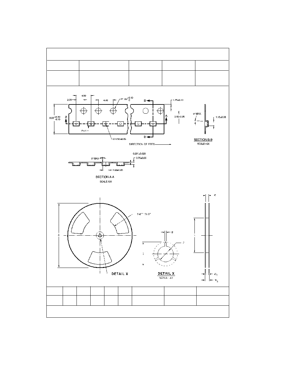
Tape and Reel Specification
TAPE FORMAT for SC70
TAPE DIMENSIONS inches (millimeters)
Package
Tape
Number
Cavity
Cover Tape
Designator
Section
Cavities
Status
Status
Leader (Start End)
125 (typ)
Empty
Sealed
P6X
Carrier
3000
Filled
Sealed
Trailer (Hub End)
75 (typ)
Empty
Sealed
9
www.fairchildsemi.com
NC7SV57
∑
NC7SV58
Tape and Reel Specification
(Continued)
TAPE FORMAT for MicroPak
TAPE DIMENSIONS inches (millimeters)
REEL DIMENSIONS inches (millimeters)
Package
Tape
Number
Cavity
Cover Tape
Designator
Section
Cavities
Status
Status
Leader (Start End)
125 (typ)
Empty
Sealed
L6X
Carrier
5000
Filled
Sealed
Trailer (Hub End)
75 (typ)
Empty
Sealed
Tape
Size
A
B
C
D
N
W1
W2
W3
8 mm
7.0
0.059
0.512
0.795
2.165
0.331
+
0.059/
-
0.000
0.567
W1
+
0.078/
-
0.039
(177.8)
(1.50)
(13.00)
(20.20)
(55.00)
(8.40
+
1.50/
-
0.00)
(14.40)
(W1
+
2.00/
-
1.00)

www.fairchildsemi.com
10
NC
7
S
V57
∑
NC
7
S
V58
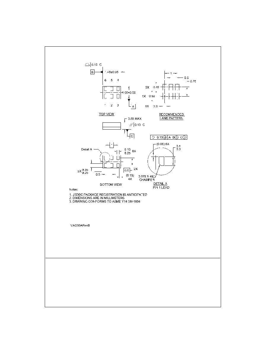
Physical Dimensions
inches (millimeters) unless otherwise noted
6-Lead SC70, EIAJ SC88, 1.25mm Wide
Package Number MAA06A
11
www.fairchildsemi.com
NC7SV57
∑
NC7SV58
T
i
nyLogi
c
ULP-
A Uni
versal
C
o
nfi
gurabl
e
2
-
I
nput
Logi
c Gat
e
s
Physical Dimensions
inches (millimeters) unless otherwise noted (Continued)
6-Lead MicroPak, 1.0mm Wide
Package Number MAC06A
Fairchild does not assume any responsibility for use of any circuitry described, no circuit patent licenses are implied and
Fairchild reserves the right at any time without notice to change said circuitry and specifications.
LIFE SUPPORT POLICY
FAIRCHILD'S PRODUCTS ARE NOT AUTHORIZED FOR USE AS CRITICAL COMPONENTS IN LIFE SUPPORT
DEVICES OR SYSTEMS WITHOUT THE EXPRESS WRITTEN APPROVAL OF THE PRESIDENT OF FAIRCHILD
SEMICONDUCTOR CORPORATION. As used herein:
1. Life support devices or systems are devices or systems
which, (a) are intended for surgical implant into the
body, or (b) support or sustain life, and (c) whose failure
to perform when properly used in accordance with
instructions for use provided in the labeling, can be rea-
sonably expected to result in a significant injury to the
user.
2. A critical component in any component of a life support
device or system whose failure to perform can be rea-
sonably expected to cause the failure of the life support
device or system, or to affect its safety or effectiveness.
www.fairchildsemi.com