© 2003 Fairchild Semiconductor Corporation
DS012171
www.fairchildsemi.com
October 1996
Revised May 2003
NC7SZ12
6 T
i
ny
Logic
U
H
S Buff
er wit
h
3-
ST
A
T
E Output
NC7SZ126
TinyLogic
UHS Buffer with 3-STATE Output
General Description
The NC7SZ126 is a single buffer with 3-STATE output from
Fairchild's Ultra High Speed Series of TinyLogic
. The
device is fabricated with advanced CMOS technology to
achieve ultra high speed with high output drive while main-
taining low static power dissipation over a very broad V
CC
operating range. The device is specified to operate over
the 1.65V to 5.5V range. The inputs and output are high
impedance above ground when V
CC
is 0V. Inputs tolerate
voltages up to 6V independent of V
CC
operating voltage.
The output tolerates voltages above V
CC
in the 3-STATE
condition.
Features
s
Space saving SOT23 or SC70 5-lead package
s
Ultra small MicroPak
leadless package
s
Ultra High Speed; t
PD
2.6 ns Typ into 50 pF at 5V V
CC
s
High Output Drive;
±
24 mA at 3V V
CC
s
Broad V
CC
Operating Range; 1.65V to 5.5V
s
Matches the performance of LCX when operated at
3.3V V
CC
s
Power down high impedance inputs/output
s
Overvoltage tolerant inputs facilitate 5V to 3V
translation
s
Patented noise/EMI reduction circuitry implemented
Ordering Code:
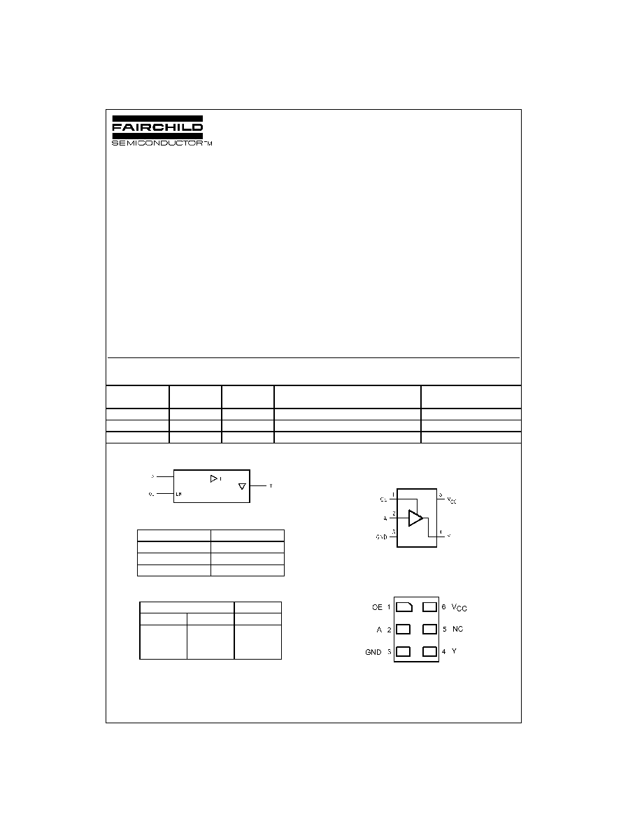
Logic Symbol
Pin Descriptions
Function Table
H
=
HIGH Logic Level
X
=
HIGH or LOW Logic Level
L
=
LOW Logic Level
Z
=
HIGH Impedance State
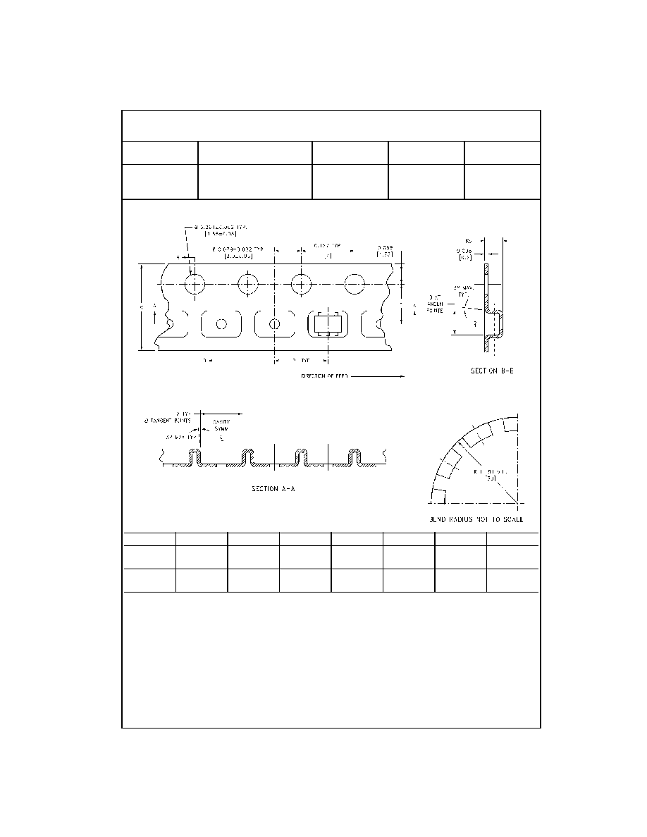
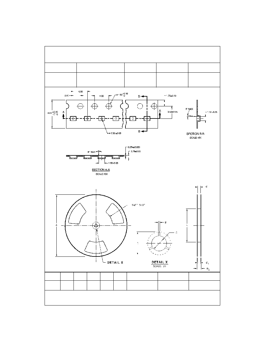
Connection Diagrams
Pin Assignments for SC70 and SOT23
(Top View)
Pad Assignments for MicroPak
(Top Thru View)
TinyLogic
is a registered trademark of Fairchild Semiconductor Corporation.
MicroPak
is a trademark of Fairchild Semiconductor Corporation.
Order Package
Product
Code
Package Description
Supplied As
Number
Number
Top Mark
NC7SZ126M5X
MA05B
7Z26
5-Lead SOT23, JEDEC MO-178, 1.6mm
3k Units on Tape and Reel
NC7SZ126P5X
MAA05A
Z26
5-Lead SC70, EIAJ SC-88a, 1.25mm Wide
3k Units on Tape and Reel
NC7SZ126L6X
MAC06A
FF
6-Lead MicroPak, 1.0mm Wide
5k Units on Tape and Reel
Pin Names
Description
A, OE
Inputs
Y
Output
NC
No Connect
Inputs
Output
OE
A
OUT Y
H
L
L
H
H
H
L
X
Z
www.fairchildsemi.com
2
NC7SZ126
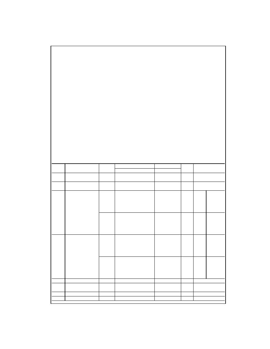
Absolute Maximum Ratings
(Note 1)
Recommended Operating
Conditions
(Note 2)
Note 1: Absolute maximum ratings are DC values beyond which the device
may be damaged or have its useful life impaired. The datasheet specifica-
tions should be met, without exception, to ensure that the system design is
reliable over its power supply, temperature, and output/input loading vari-
ables. Fairchild does not recommend operation outside datasheet specifi-
cations.
Note 2: Unused inputs must be held HIGH or LOW. They may not float.
DC Electrical Characteristics
Supply Voltage (V
CC
)
-
0.5V to
+
6V
DC Input Voltage (V
IN
)
-
0.5V to
+
6V
DC Output Voltage (V
OUT
)
-
0.5V to
+
6V
DC Input Diode Current (I
IK
)
@V
IN
<
-
0.5V
-
50 mA
@ V
IN
>
6V
+
20 mA
DC Output Diode Current (I
OK
)
@V
OUT
<
-
0.5V
-
50 mA
@ V
OUT
>
6V, V
CC
=
GND
+
20 mA
DC Output Current (I
OUT
)
±
50 mA
DC V
CC
/GND Current (I
CC
/I
GND
)
±
50 mA
Storage Temperature (T
STG
)
-
65
∞
C to
+
150
∞
C
Junction Temperature under Bias (T
J
)
150
∞
C
Junction Lead Temperature (T
L
);
(Soldering, 10 seconds)
260
∞
C
Power Dissipation (P
D
) @
+
85
∞
C
SOT23-5
200 mW
SC70-5
150 mW
Supply Voltage Operating (V
CC
)
1.65V to 5.5V
Supply Voltage Data Retention (V
CC
)
1.5V to 5.5V
Input Voltage (V
IN
)
0V to 5.5V
Output Voltage (V
OUT
)
Active State
0V to V
CC
3-State
0V to 5.5V
Operating Temperature (T
A
)
-
40
∞
C to
+
85
∞
C
Input Rise and Fall Time (t
r
, t
f
)
V
CC
=
1.8V, 2.5V
±
0.2V
0 ns/V to 20 ns/V
V
CC
=
3.3V
±
0.3V
0 ns/V to 10 ns/V
V
CC
=
5.0V
±
0.5V
0 ns/V to 5 ns/V
Thermal Resistance (
JA
)
SOT23-5
300
∞
C/W
SC70-5
425
∞
C/W
Symbol
Parameter
V
CC
T
A
=
+
25
∞
C
T
A
=
-
40
∞
C to
+
85
∞
C
Unit
Conditions
(V)
Min
Typ
Max
Min
Max
V
IH
HIGH Level Input Voltage
1.65 to 1.95 0.75 V
CC
0.75 V
CC
V
.
2.3 to 5.5
0.7 V
CC
0.7 V
CC
V
IL
LOW Level Input Voltage
1.65 to 1.95
0.25 V
CC
0.25 V
CC
V
2.3 to 5.5
0.3 V
CC
0.3 V
CC
V
OH
HIGH Level Output Voltage
1.65
1.55
1.65
1.55
V
V
IN
=
V
IH
I
OH
=
-
100
µ
A
1.8
1.7
1.8
1.7
2.3
2.2
2.3
2.2
3.0
2.9
3.0
2.9
4.5
4.4
4.5
4.4
1.65
1.29
1.52
1.29
V
I
OH
=
-
4 mA
2.3
1.9
2.15
1.9
I
OH
=
-
8 mA
3.0
2.4
2.80
2.4
I
OH
=
-
16 mA
3.0
2.3
2.68
2.3
I
OH
=
-
24 mA
4.5
3.8
4.20
3.8
I
OH
=
-
32 mA
V
OL
LOW Level
1.65
0.0
0.1
0.1
V
V
IN
=
V
IL
I
OL
=
100
µ
A
Output Voltage
1.8
0.0
0.1
0.1
2.3
0.0
0.1
0.1
3.0
0.0
0.1
0.1
4.5
0.0
0.1
0.1
1.65
0.08
0.24
0.24
V
I
OL
=
4 mA
2.3
0.10
0.3
0.3
I
OL
=
8 mA
3.0
0.15
0.4
0.4
I
OL
=
16 mA
3.0
0.22
0.55
0.55
I
OL
=
24 mA
4.5
0.22
0.55
0.55
I
OL
=
32 mA
I
IN
Input Leakage Current
0 to 5.5
±
1
±
10
µ
A
V
IN
=
5.5V, GND
I
OZ
3-STATE
0 to 5.5
±
1
±
10
µ
A
V
IN
=
V
IH
or V
IL
Output Leakage
V
O
=
V
CC
or GND
I
OFF
Power Off Leakage Current
0.0
1
10
µ
A
V
IN
or V
OUT
=
5.5V
I
CC
Quiescent Supply Current
1.65 to 5.5
2.0
20
µ
A
V
IN
=
5.5V, GND
3
www.fairchildsemi.com
NC7SZ12
6
AC Electrical Characteristics
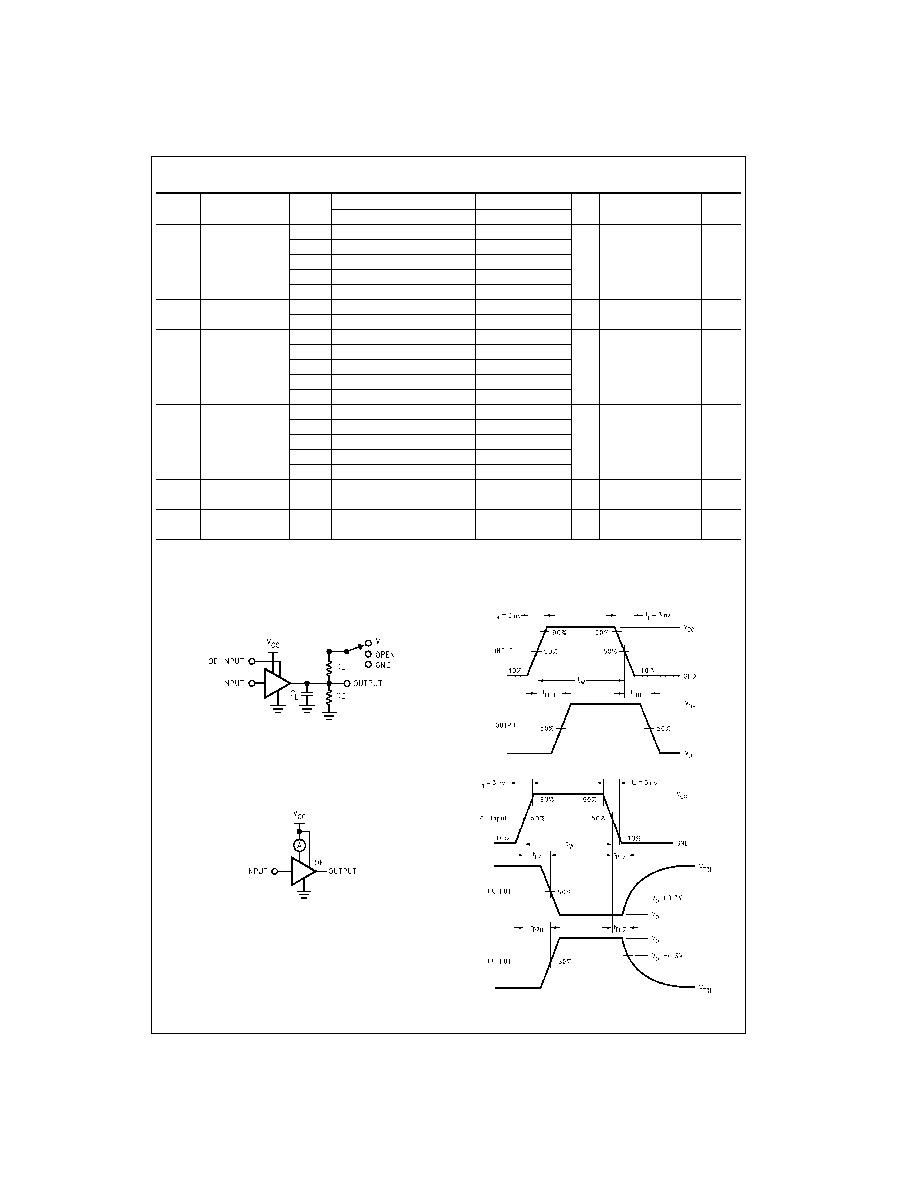
Note 3: C
PD
is defined as the value of the internal equivalent capacitance which is derived from dynamic operating current consumption (I
CCD
) at no output
loading and operating at 50% duty cycle. (See Figure 2.) C
PD
is related to I
CCD
dynamic operating current by the expression:
I
CCD
=
(CPD) (V
CC
) (f
IN
)
+
(I
CC
static).
AC Loading and Waveforms
C
L
includes load and stray capacitance
Input PRR
=
1.0 MHz, t
w
=
500 ns
FIGURE 1. AC Test Circuit
Input
=
AC Waveform; t
r
=
t
f
=
1.8 ns;
PRR
=
10 MHz; Duty Cycle
=
50%
FIGURE 2. I
CCD
Test Circuit
FIGURE 3. AC Waveforms
Symbol
Parameter
V
CC
T
A
=
+
25
∞
C
T
A
=
-
40
∞
C to
+
85
∞
C
Units
Conditions
Fig. No.
(V)
Min
Typ
Max
Min
Max
t
PLH
Propagation Delay
1.65
2.0
6.4
13.2
2.0
13.8
ns
Figures
1, 3
t
PHL
1.8
2
5.3
11
2
11.5
2.5
±
0.2
0.8
3.4
7.5
0.8
8.0
C
L
=
15 pF, RD
=
1 M
3.3
±
0.3
0.5
2.5
5.2
0.5
5.5
S
1
=
OPEN
5.0
±
0.5
0.5
2.1
4.5
0.5
4.8
t
PLH
Propagation Delay
3.3
±
0.3
1.5
3.2
5.7
1.5
6.0
ns
C
L
=
50 pF, RD
=
500
Figures
1, 3
t
PHL
5.0
±
0.5
0.8
2.6
5.0
0.8
5.3
S
1
=
OPEN
t
PZL
Output Enable Time
1.65
2.0
8.4
15.0
2.0
15.6
ns
C
L
=
50 pF, RD
=
500
,
Figures
1, 3
t
PZH
1.8
2.0
6.1
11.5
2
12
RU
=
500
2.5
±
0.2
1.5
3.8
8.0
1.5
8.5
S
1
=
GND for t
PZH
3.3
±
0.3
1.5
3.2
5.7
1.5
6.0
S
1
=
V
I
for t
PZL
5.0
±
0.5
0.8
2.3
5.0
0.8
5.3
V
I
=
2
◊
V
CC
t
PLZ
Output Disable Time
1.65
2.0
6.5
13.2
2.0
14.5
ns
C
L
=
50 pF, RD
=
500
,
Figures
1, 3
t
PHZ
1.8
2.0
5.6
11
2.0
12
RU
=
500
2.5
±
0.2
1.0
4.0
8.0
1.0
8.5
S
1
=
GND for t
PHZ
3.3
±
0.3
1.0
3.5
5.7
1.0
6.0
S
1
=
V
I
for t
PLZ
5.0
±
0.5
0.5
2.5
4.7
0.5
5.0
V
I
=
2
◊
V
CC
C
IN
Input Capacitance
0
4
pF
C
OUT
Output Capacitance
0
8
C
PD
Power Dissipation
3.3
17
pF
(Note 3)
Figure 2
Capacitance
5.0
24