© 2003 Fairchild Semiconductor Corporation
DS012176
www.fairchildsemi.com
October 1996
Revised May 2003
NC7SZ14
T
i
nyL
ogic
UHS Inve
rte
r
w
i
th Schm
it
t T
r
i
gger In
put
NC7SZ14
TinyLogic
UHS Inverter with Schmitt Trigger Input
General Description
The NC7SZ14 is a single Inverter with Schmitt Trigger
input from Fairchild's Ultra High Speed Series of
TinyLogic
. The device is fabricated with advanced CMOS
technology to achieve ultra high speed with high output
drive while maintaining low static power dissipation over a
very broad V
CC
operating range. The device is specified to
operate over the 1.65V to 5.5V V
CC
range. The input and
output are high impedance when V
CC
is 0V. Inputs tolerate
voltages up to 6V independent of V
CC
operating voltage.
Features
s
Space saving SOT23 or SC70 5-lead package
s
Ultra small MicroPak
leadless package
s
Ultra High Speed; t
PD
3.7 ns Typ into 50 pF at 5V V
CC
s
High Output Drive;
±
24 mA at 3V V
CC
s
Broad V
CC
Operating Range; 1.65V to 5.5V
s
Matches the performance of LCX when operated at
3.3V V
CC
s
Power down high impedance inputs/output
s
Overvoltage Tolerant inputs facilitate 5V to 3V
translation
s
Patented noise/EMI reduction circuitry implemented
Ordering Code:
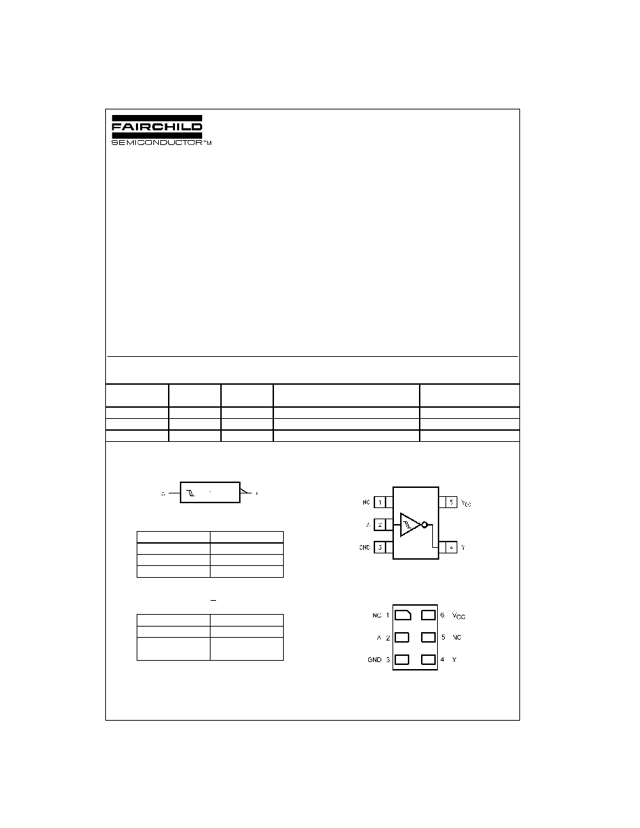
Logic Symbol
IEEE/IEC
Pin Descriptions
Function Table
Y
=
A
H
=
HIGH Logic Level
L
=
LOW Logic Level
Connection Diagrams
Pin Assignments for SOT23 and SC70
(Top View)
Pad Assignments for MicroPak
(Top Thru View)
TinyLogic
is a registered trademark of Fairchild Semiconductor Corporation.
MIcroPak
is a trademark of Fairchild Semiconductor Corporation.
Order Package
Product
Code
Package Description
Supplied As
Number
Number
Top Mark
NC7SZ14M5X
MA05B
7Z14
5-Lead SOT23, JEDEC MO-178, 1.6mm
3k Units on Tape and Reel
NC7SZ14P5X
MAA05A
Z14
5-Lead SC70, EIAJ SC-88a, 1.25mm Wide
3k Units on Tape and Reel
NC7SZ14L6X
MAC06A
B6
6-Lead MicroPak, 1.0mm Wide
5k Units on Tape and Reel
Pin Names
Description
A
Input
Y
Output
NC
No Connect
Input
Output
A
Y
L
H
H
L
www.fairchildsemi.com
2
NC7SZ14
Absolute Maximum Ratings
(Note 1)
Recommended Operating
Conditions
(Note 2)
Note 1: Absolute maximum ratings are DC values beyond which the device
may be damaged or have its useful life impaired. The datasheet specifica-
tion should be met, without exception, to ensure that the system design is
reliable over its power supply, temperature, and output/input loading vari-
ables. Fairchild does not recommend operation outside datasheet specifi-
cations.
Note 2: Unused inputs must be held HIGH or LOW. They may not float.
DC Electrical Characteristics
Supply Voltage (V
CC
)
-
0.5V to
+
6V
DC Input Voltage (V
IN
)
-
0.5V to
+
6V
DC Output Voltage (V
OUT
)
-
0.5V to
+
6V
DC Input Diode Current (I
IK
)
@V
IN
<
-
0.5V
-
50 mA
@V
IN
>
6V
+
20 mA
DC Output Diode Current (I
OK
)
@V
OUT
<
-
0.5V
-
50 mA
@V
OUT
>
6V, V
CC
=
GND
+
20 mA
DC Output Current (I
OUT
)
±
50 mA
DC V
CC
/GND Current (I
CC
/I
GND
)
±
50 mA
Storage Temperature (T
STG
)
-
65
∞
C to
+
150
∞
C
Junction Temperature under Bias (T
J
)
150
∞
C
Junction Lead Temperature (T1);
(Soldering, 10 seconds)
260
∞
C
Power Dissipation (P
D
) @
+
85
∞
C
SOT23-5
200 mW
SC70-5
150 mW
Supply Voltage Operating (V
CC
)
1.65V to 5.5V
Supply Voltage Data Retention (V
CC
)
1.5V to 5.5V
Input Voltage (V
IN
)
0V to 5.5V
Output Voltage (V
OUT
)
0V to V
CC
Operating Temperature (T
A
)
-
40
∞
C to
+
85
∞
C
Thermal Resistance (
JA
)
SOT23-5
300
∞
C/W
SC70-5
425
∞
C/W
Symbol
Parameter
V
CC
T
A
=
+
25
∞
C
T
A
=
-
40
∞
C to
+
85
∞
C
Unit
Conditions
(V)
Min
Typ
Max
Min
Max
V
P
Positive Threshold
1.65
0.6
1.0
1.4
0.6
1.4
V
Voltage
1.8
0.7
1.1
1.5
0.7
1.5
2.3
1.0
1.4
1.8
1.0
1.8
3.0
1.3
1.75
2.2
1.3
2.2
4.5
1.9
2.45
3.1
1.9
3.1
5.5
2.2
2.9
3.6
2.2
3.6
V
N
Negative Threshold
1.65
0.2
0.5
0.8
0.2
0.8
V
Voltage
1.8
0.25
0.55
0.9
0.25
0.9
2.3
0.40
0.75
1.15
0.40
1.15
3.0
0.6
1.0
1.5
0.6
1.5
4.5
1.0
1.43
2.0
1.0
2.0
5.5
1.2
1.70
2.3
1.2
2.3
V
H
Hysteresis Voltage
1.65
0.1
0.48
0.9
0.1
0.9
V
1.8
0.15
0.54
1.0
0.15
1.0
2.3
0.25
0.65
1.1
0.25
1.1
3.0
0.4
0.77
1.2
0.4
1.2
4.5
0.6
1.01
1.5
0.6
1.5
5.5
0.7
1.18
1.7
0.7
1.7
V
OH
HIGH Level
1.65
1.55
1.65
1.55
V
V
IN
=
V
IL
I
OH
=
-
100
µ
A
Output Voltage
1.8
1.7
1.8
1.7
2.3
2.2
2.3
2.2
3.0
2.9
3.0
2.9
4.5
4.4
4.5
4.4
1.65
1.29
1.52
1.29
V
I
OH
=
-
4 mA
2.3
1.9
2.15
1.9
I
OH
=
-
8 mA
3.0
2.4
2.80
2.4
I
OH
=
-
16 mA
3.0
2.3
2.68
2.3
I
OH
=
-
24 mA
4.5
3.8
4.20
3.8
I
OH
=
-
32 mA
3
www.fairchildsemi.com
NC7SZ14
DC Electrical Characteristics
(Continued)
AC Electrical Characteristics
Note 3: C
PD
is defined as the value of the internal equivalent capacitance which is derived from dynamic operating current consumption (I
CCD
) at no output
loading and operating at 50% duty cycle. (See Figure 2.) C
PD
is related to I
CCD
dynamic operating current by the expression:
I
CCD
=
(C
PD
) (V
CC
) (f
IN
)
+
(I
CC
static).
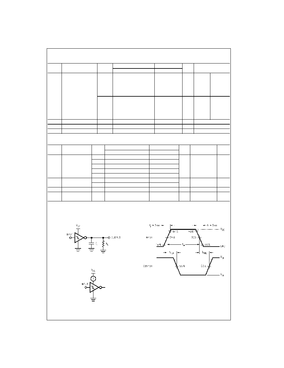
AC Loading and Waveforms
C
L
includes load and stray capacitance
Input PRR
=
1.0 MHz; t
w
=
500 ns
FIGURE 1. AC Test Circuit
Input
=
AC Waveform; t
r
=
t
f
=
1.8 ns
PRR
=
10 MHz; Duty Cycle
=
50%
FIGURE 2. I
CCD
Test Circuit
FIGURE 3. AC Waveforms
Symbol
Parameter
V
CC
T
A
=
+
25
∞
C
T
A
=
-
40
∞
C to
+
85
∞
C
Unit
Conditions
(V)
Min
Typ
Max
Min
Max
V
OL
LOW Level
1.65
0.0
0.1
0.1
V
V
IN
=
V
IH
I
OL
=
100
µ
A
Output Voltage
1.8
0.0
0.1
0.1
2.3
0.0
0.1
0.1
3.0
0.0
0.1
0.1
4.5
0.0
0.1
0.1
1.65
0.08
0.24
0.24
V
I
OL
=
4 mA
2.3
0.10
0.3
0.3
I
OL
=
8 mA
3.0
0.15
0.4
0.4
I
OL
=
16 mA
3.0
0.22
0.55
0.55
I
OL
=
24 mA
4.5
0.22
0.55
0.55
I
OL
=
32 mA
I
IN
Input Leakage Current
0 to 5.5
±
1
±
10
µ
A
V
IN
=
5.5V, GND
I
OFF
Power Off Leakage Current
0.0
1
10
µ
A
V
IN
or V
OUT
=
5.5V
I
CC
Quiescent Supply Current
1.65 to 5.5
2.0
20
µ
A
V
IN
=
5.5V, GND
Symbol
Parameter
V
CC
T
A
=
+
25
∞
C
T
A
=
-
40
∞
C to
+
85
∞
C
Unit
Conditions
Figure
(V)
Min
Typ
Max
Min
Max
Number
t
PLH
,
Propagation Delay
1.65
2.0
9.1
15.0
2.0
15.6
ns
Figures
1, 3
t
PHL
1.8
2.0
7.6
12.5
2.0
13
2.5
±
0.2
1.0
5.0
9.0
1.0
9.5
C
L
=
15 pF,
3.3
±
0.3
1.0
3.7
6.3
1.0
6.5
R
L
=
1 M
5.0
±
0.5
0.5
3.1
5.2
0.5
5.5
t
PLH
,
Propagation Delay
3.3
±
0.3
1.5
4.4
7.2
1.5
7.5
ns
C
L
=
50 pF,
Figures
1, 3
t
PHL
5.0
±
0.5
0.8
3.7
5.9
0.8
6.2
R
L
=
500
C
IN
Input Capacitance
0
4
pF
C
PD
Power Dissipation
3.3
24
pF
(Note 3)
Figure 2
Capacitance
5.0
30