© 2003 Fairchild Semiconductor Corporation
DS500158
www.fairchildsemi.com
May 1998
Revised May 2003
NC7SZ17
5 T
i
ny
Logic
U
H
S D-T
y
pe Fl
ip-
F
lop wit
h
Async
h
ronous Clea
r
NC7SZ175
TinyLogic
UHS D-Type Flip-Flop
with Asynchronous Clear
General Description
The NC7SZ175 is a single positive edge-triggered D-type
CMOS Flip-Flop with Asynchronous Clear from Fairchild's
Ultra High Speed Series of TinyLogic
in the space saving
SC70 6-lead package. The device is fabricated with
advanced CMOS technology to achieve ultra high speed
with high output drive while maintaining low static power
dissipation over a very broad V
CC
operating range. The
device is specified to operate over the 1.65V to 5.5V V
CC
range. The inputs and output are high impedance when
V
CC
is 0V. Inputs tolerate voltages up to 7V independent of
V
CC
operating voltage. This single flip-flop will store the
state of the D input that meets the setup and hold time
requirements on the LOW-to-HIGH Clock (CP) transition. A
LOW input to Clear sets the Q output to LOW level. The
Clear input is independent of clock.
Features
s
Space saving SC70 6-lead package
s
Ultra small MicroPak
leadless package
s
Ultra High Speed; t
PD
2.6 ns Typ into 50 pF at 5V V
CC
s
High Output Drive;
±
24 mA at 3V V
CC
s
Broad V
CC
Operating Range; 1.65V to 5.5V
s
Matches the performance of LCX when operated at
3.3V V
CC
s
Power down high impedance inputs/output
s
Overvoltage tolerant inputs facilitate 5V to 3V translation
s
Patented noise/EMI reduction circuitry implemented
Ordering Code:
TinyLogic
is a registered trademark of Fairchild Semiconductor Corporation.
MicroPak
is a trademark of Fairchild Semiconductor Corporation.
Order Package
Product
Code
Package Description
Supplied As
Number
Number
Top Mark
NC7SZ175P6X
MAA06A
Z75
6-Lead SC70, EIAJ SC88, 1.25mm Wide 3k Units on Tape and Reel
NC7SZ175L6X
MAC06A
C4
6-Lead MicroPak, 1.0mm Wide
5k Units on Tape and Reel
www.fairchildsemi.com
2
NC7SZ175
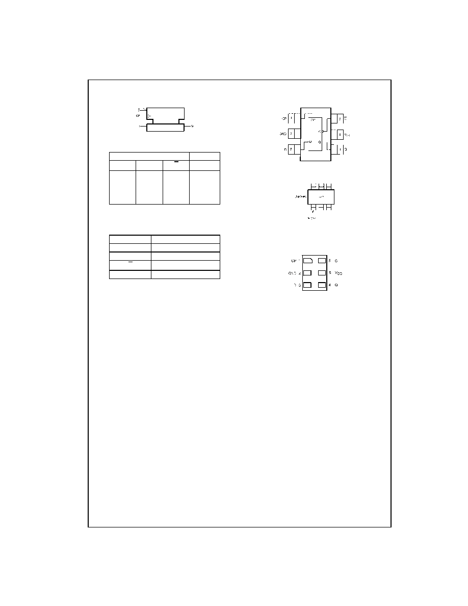
Logic Symbol
IEEE/IEC
Function Table
H
=
HIGH Logic Level
Qn
=
No change in data
L
=
LOW Logic Level
X
=
Immaterial
Pin Descriptions
Connection Diagrams
Pin Assignments for SC70
(Top View)
Pin One Orientation Diagram
AAA represents Product Code Top Mark - see ordering code
Note: Orientation of Top Mark determines Pin One location. Read the top
product code mark left to right, Pin One is the lower left pin (see diagram).
Pad Assignments for MicroPak
(Top Thru View)
Inputs
Output
CP
D
C
Q
L
H
L
H
H
H
X
H
Qn
X
X
L
L
Pin Names
Description
D
Data Input
CP
Clock Pulse Input
C
Clear Input
Q
Flip-Flop Output
3
www.fairchildsemi.com
NC7SZ17
5
Absolute Maximum Ratings
(Note 1)
Recommended Operating
Conditions
(Note 2)
Note 1: The "Absolute Maximum Ratings": are those values beyond which
the safety of the device cannot be guaranteed. The device should not be
operated at these limits. The parametric values defined in the Electrical
Characteristics tables are not guaranteed at the absolute maximum ratings.
The "Recommended Operating Conditions" table will define the conditions
for actual device operation.
Note 2: Unused inputs must be held HIGH or LOW. They may not float.
DC Electrical Characteristics
Supply Voltage (V
CC
)
-
0.5V to
+
7.0V
DC Input Voltage (V
IN
)
-
0.5V to
+
7.0V
DC Output Voltage (V
OUT
)
-
0.5V to
+
7.0V
DC Input Diode Current (I
IK
)
V
IN
<
0V
-
50 mA
DC Output Diode Current (I
OK
)
V
OUT
<
0V
-
50 mA
DC Output (I
OUT
) Source/Sink Current
±
50 mA
DC V
CC
/GND Current (I
CC
/I
GND
)
±
50 mA
Storage Temperature Range (T
STG
)
-
65
∞
C to
+
150
∞
C
Junction Temperature under Bias (T
J
)
150
∞
C
Junction Lead Temperature (T
L
)
(Soldering, 10 seconds)
260
∞
C
Power Dissipation (P
D
) @
+
85
∞
C
180 mW
Power Supply
Operating (V
CC
)
1.65V to 5.5V
Data Retention
1.5V to 5.5V
Input Voltage (V
IN
)
0V to 5.5V
Output Voltage (V
OUT
)
0V to V
CC
Input Rise and Fall Time (t
r
, t
f
)
V
CC
=
1.8V, 2.5V
±
0.2V
0 to 20 ns/V
V
CC
=
3.3V
±
0.3V
0 to 10 ns/V
V
CC
=
5.5V
±
0.5V
0 to 5 ns/V
Operating Temperature (T
A
)
-
40
∞
C to
+
85
∞
C
Thermal Resistance (
JA
)
350
∞
C/W
Symbol
Parameter
V
CC
T
A
=
+
25
∞
C
T
A
=
-
40
∞
C to
+
85
∞
C
Unit
Conditions
(V)
Min
Typ
Max
Min
Max
V
IH
HIGH Level Control
1.65 to 1.95 0.75 V
CC
0.75 V
CC
V
Input Voltage
2.3 to 5.5
0.7 V
CC
0.7 V
CC
V
IL
LOW Level Control
1.65 to 1.95
0.25 V
CC
0.25 V
CC
V
Input Voltage
2.3 to 5.5
0.3 V
CC
0.3 V
CC
V
OH
HIGH Level Control
1.65
1.55
1.65
1.55
V
I
OH
=
-
100
µ
A
Output Voltage
1.8
1.7
1.8
1.7
2.3
2.2
2.3
2.2
3.0
2.9
3.0
2.9
4.5
4.4
4.5
4.4
V
IN
=
V
IH
1.65
1.24
1.52
1.29
or V
IL
I
OH
=
-
4 mA
2.3
1.9
2.15
1.9
I
OH
=
-
8 mA
3.0
2.4
2.8
2.4
I
OH
=
-
16 mA
3.0
2.3
2.68
2.3
I
OH
=
-
24 mA
4.5
3.8
4.2 3.8
I
OH
=
-
32 mA
V
OL
LOW Level Control
1.65
0.0
0.1
0.1
V
I
OL
=
100
µ
A
Output Voltage
1.8
0.0
0.1
0.1
2.3
0.0
0.1
0.1
3.0
0.0
0.1
0.1
4.5
0.0
0.1
0.1
V
IN
=
V
IL
1.65
0.08
0.24
0.24
or V
IH
I
OL
=
4 mA
2.3
0.10
0.3
0.3
I
OL
=
8 mA
3.0
0.15
0.4
0.4
I
OL
=
16 mA
3.0
0.22
0.55
0.55
I
OL
=
24 mA
4.5
0.22
0.55
0.55
I
OL
=
32 mA
I
IN
Input Leakage Current
0 to 5.5
±
0.1
±
1.0
µ
A
0
V
IN
5.5V
I
OFF
Power Off Leakage Current
0.0
1.0
10
µ
A
V
IN
or V
OUT
=
5.5V
I
CC
Quiescent Supply Current
1.65 to 5.5
1.0
10.0
µ
A
V
IN
=
5.5V, GND
www.fairchildsemi.com
4
NC7SZ175
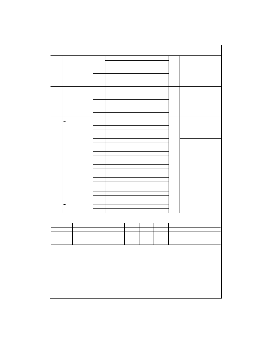
AC Electrical Characteristics
Capacitance
(Note 3)
Note 3: T
A
=
+
25C, f
=
1MHz.
Note 4: C
PD
is defined as the value of the internal equivalent capacitance which is derived from dynamic operating current consumption (I
CCD
) at no output
loading and operating at 50% duty cycle. (See Figure 2)
C
PD
is related to I
CCD
dynamic operating current by the expression: I
CCD
=
(C
PD
)(V
CC
)(f
IN
)
+
(I
CC
static).
Symbol
Parameter
V
CC
T
A
=
+
25
∞
C
T
A
=
-
40
∞
C to
+
85
∞
C
Units
Conditions
Figure
(V)
Min
Typ Max
Min
Max
Number
f
MAX
Maximum Clock
1.65
100
MHz
Figures
1, 4
Frequency
1.8
100
2.5
±
0.2
125
C
L
=
50 pF
3.3
±
0.3
150
R
L
=
500
5.0
±
0.5
175
t
PLH
Propagation Delay
1.65
2.5
9.8
15.0
2.5
16.5
ns
Figures
1, 3
t
PHL
CP to Q
1.8
2.5
6.5
10.0
2.5
11.0
2.5
±
0.2
2.0
3.8
6.5
2.0
7.0
C
L
=
15 pF
3.3
±
0.3
1.5
2.8
4.5
1.4
5.0
R
L
=
1 M
5.0
±
0.5
1.0
2.2
3.5
1.0
3.8
3.3
±
0.3
2.0
3.4
5.5
1.6
6.2
C
L
=
50 pF
Figures
1, 3
5.0
±
0.5
1.5
2.6
4.0
1.4
4.7
R
L
=
500
t
PHL
Propagation Delay
1.65
2.5
9.8
13.5
2.5
15.0
ns
Figures
1, 3
C to Q
1.8
2.5
6.5
9.0
2.5
10.0
2.5
±
0.2
2.0
3.8
6.0
2.0
6.4
C
L
=
15 pF
3.3
±
0.3
1.5
2.8
4.3
1.2
4.6
R
L
=
1 M
5.0
±
0.5
1.5
2.2
3.2
1.0
3.5
3.3
±
0.3
1.5
3.4
5.3
1.5
5.8
C
L
=
50 pF
Figures
1, 3
5.0
±
0.5
1.0
2.7
4.0
1.2
4.5
R
L
=
500
t
S
Setup Time
2.5
±
0.2
2.5
ns
C
L
=
50 pF
Figures
1, 4
CP to D
3.3
±
0.3
2.0
R
L
=
500
5.0
±
0.5
1.5
t
H
Hold Time,
2.5
±
0.2
1.5
ns
C
L
=
50 pF
Figures
1, 4
CP to D
3.3
±
0.3
1.5
R
L
=
500
5.0
±
0.5
1.5
t
W
Pulse Width, CP
2.5
±
0.2
3.0
C
L
=
50 pF
Figures
1, 4
3.3
±
0.3
2.8
ns
R
L
=
500
5.0
±
0.5
2.5
Pulse Width, C
2.5
±
0.2
3.0
Clock HIGH or LOW
Figures
1, 4
3.3
±
0.3
2.8
ns
C
L
=
50 pF
5.0
±
0.5
2.5
R
L
=
500
t
rec
Recovery Time,
2.5
±
0.2
1.0
C
L
=
50 pF
Figures
1, 4
C to CP
3.3
±
0.3
1.0
ns
R
L
=
500
5.0
±
0.5
1.0
Symbol
Parameter
Typ
Max
Units
Conditions
C
IN
Input Capacitance
3
pF
V
CC
=
Open, V
IN
=
0V or V
CC
C
OUT
Output Capacitance
4
pF
V
CC
=
3.3V, V
IN
=
0V or V
CC
C
PD
Power Dissipation Capacitance
10
pF
V
CC
=
3.3V
(Note 4)
12
V
CC
=
5.0V
5
www.fairchildsemi.com
NC7SZ17
5
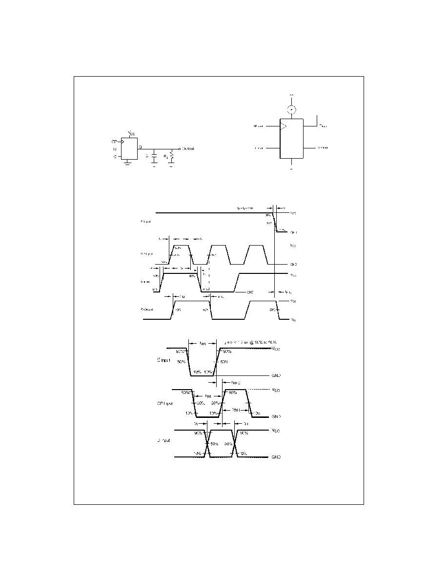
AC Loading and Waveforms
C
L
includes load and stray capacitance
Input PRR
=
1.0 MHz, t
w
=
500 ns
FIGURE 1. AC Test Circuit
CP Input
=
AC Waveform; t
r
=
t
f
=
1.8 ns;
CP Input PRR
=
10 MHz; Duty Cycle
=
50%
D Input PRR
=
5MHz; Duty Cycle
=
50%
FIGURE 2. I
CCD
Test Circuit
FIGURE 3. AC Waveforms
FIGURE 4. AC Waveforms
www.fairchildsemi.com
6
NC7SZ175
Tape and Reel Specification
TAPE FORMAT for SC70
TAPE DIMENSIONS inches (millimeters)
Package
Tape
Number
Cavity
Cover Tape
Designator
Section
Cavities
Status
Status
Leader (Start End)
125 (typ)
Empty
Sealed
P6X
Carrier
3000
Filled
Sealed
Trailer (Hub End)
75 (typ)
Empty
Sealed
Package
Tape Size
DIM A
DIM B
DIM F
DIM K
o
DIM P1
DIM W
SC70-6
8 mm
0.093
0.096
0.138
±
0.004 0.053
±
0.004
0.157
0.315
±
0.004
(2.35)
(2.45)
(3.5
±
0.10)
(1.35
±
0.10)
(4)
(8
±
0.1)
7
www.fairchildsemi.com
NC7SZ17
5
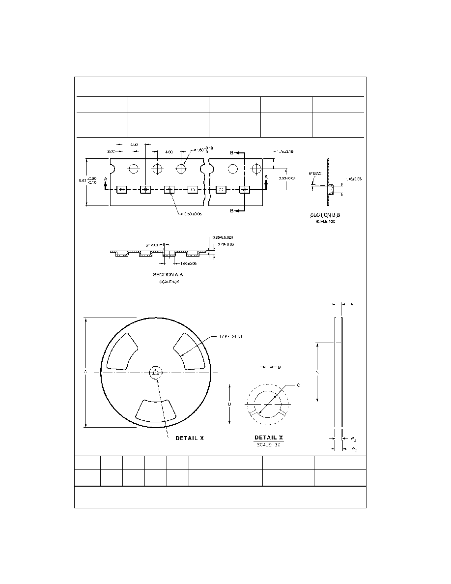
Tape and Reel Specification
(Continued)
TAPE FORMAT for MicroPak
REEL DIMENSIONS inches (millimeters)
Package
Tape
Number
Cavity
Cover Tape
Designator
Section
Cavities
Status
Status
Leader (Start End)
125 (typ)
Empty
Sealed
L6X
Carrier
5000
Filled
Sealed
Trailer (Hub End)
75 (typ)
Empty
Sealed
Tape
Size
A
B
C
D
N
W1
W2
W3
8 mm
7.0
0.059
0.512
0.795
2.165
0.331
+
0.059/
-
0.000
0.567
W1
+
0.078/
-
0.039
(177.8)
(1.50)
(13.00)
(20.20)
(55.00)
(8.40
+
1.50/
-
0.00)
(14.40)
(W1
+
2.00/
-
1.00)
www.fairchildsemi.com
8
NC7SZ175
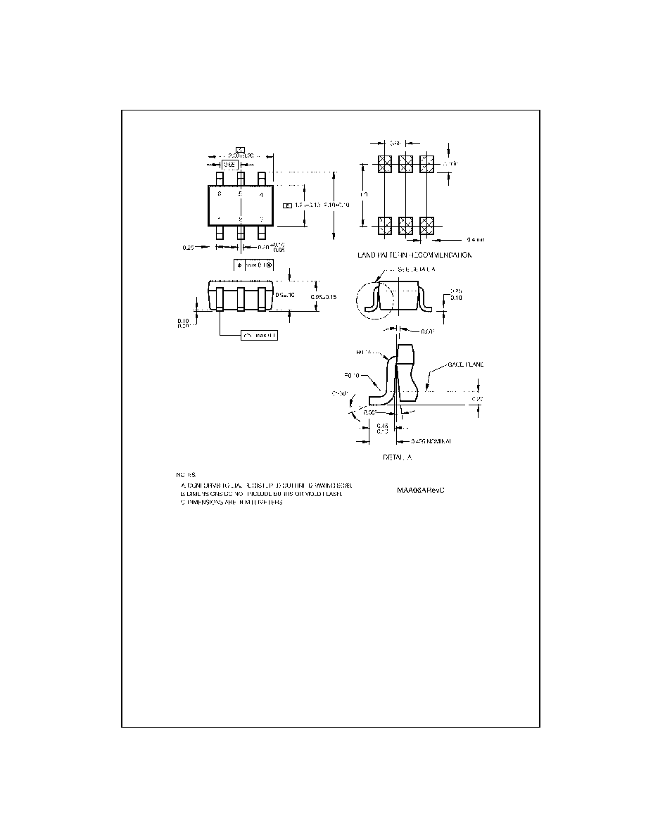
Physical Dimensions
inches (millimeters) unless otherwise noted
6-Lead SC70, EIAJ SC88, 1.25mm Wide
Package Number MAA06A
9
www.fairchildsemi.com
NC7SZ17
5 T
i
ny
Logic
U
H
S D-T
y
pe Fl
ip-
F
lop wit
h
Async
h
ronous Clea
r
Physical Dimensions
inches (millimeters) unless otherwise noted (Continued)
6-Lead MicroPak, 1.0mm Wide
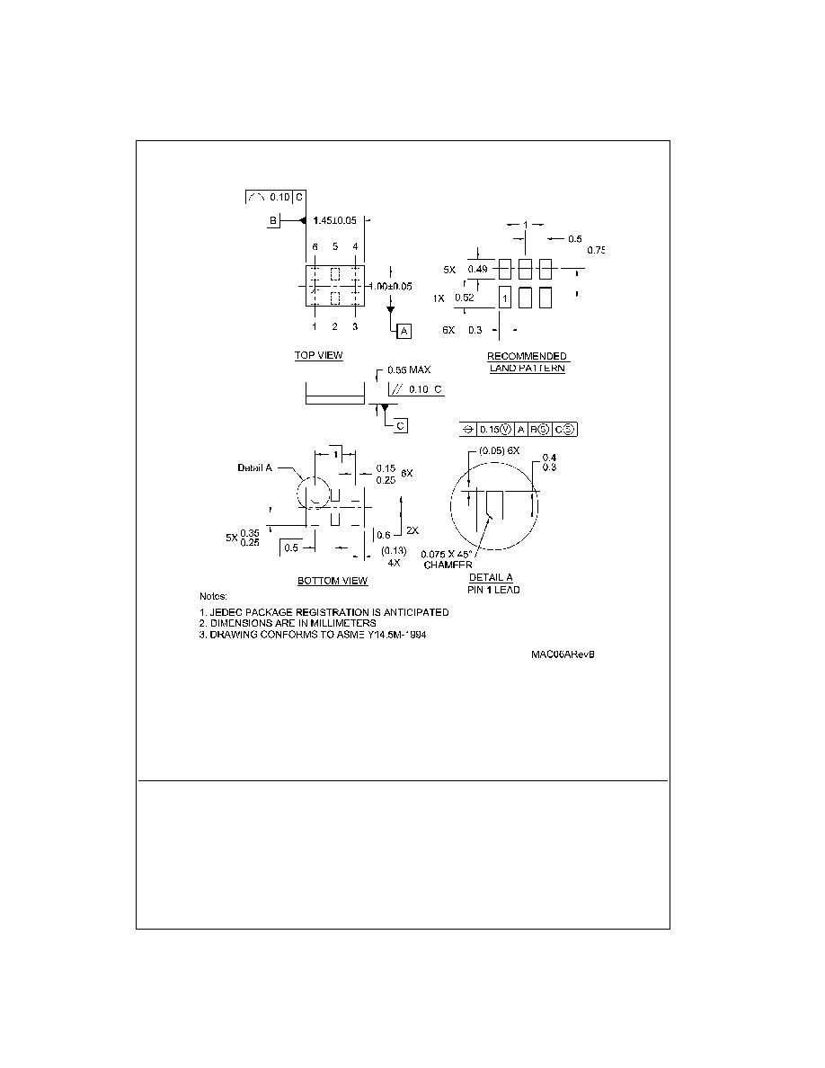
Package Number MAC06A
Fairchild does not assume any responsibility for use of any circuitry described, no circuit patent licenses are implied and
Fairchild reserves the right at any time without notice to change said circuitry and specifications.
LIFE SUPPORT POLICY
FAIRCHILD'S PRODUCTS ARE NOT AUTHORIZED FOR USE AS CRITICAL COMPONENTS IN LIFE SUPPORT
DEVICES OR SYSTEMS WITHOUT THE EXPRESS WRITTEN APPROVAL OF THE PRESIDENT OF FAIRCHILD
SEMICONDUCTOR CORPORATION. As used herein:
1. Life support devices or systems are devices or systems
which, (a) are intended for surgical implant into the
body, or (b) support or sustain life, and (c) whose failure
to perform when properly used in accordance with
instructions for use provided in the labeling, can be rea-
sonably expected to result in a significant injury to the
user.
2. A critical component in any component of a life support
device or system whose failure to perform can be rea-
sonably expected to cause the failure of the life support
device or system, or to affect its safety or effectiveness.
www.fairchildsemi.com