 | –≠–ª–µ–∫—Ç—Ä–æ–Ω–Ω—ã–π –∫–æ–º–ø–æ–Ω–µ–Ω—Ç: NC7SZ58 | –°–∫–∞—á–∞—Ç—å:  PDF PDF  ZIP ZIP |
© 2003 Fairchild Semiconductor Corporation
DS500358
www.fairchildsemi.com
April 2000
Revised May 2003
NC7SZ57
∑
N
C
7SZ5
8 T
i
ny
Logic
UH
S Unive
r
sal
Conf
igur
abl
e
2-
Input
Logic Gates
NC7SZ57 ∑ NC7SZ58
TinyLogic
UHS Universal Configurable 2-Input
Logic Gates
General Description
The NC7SZ57 and the NC7SZ58 are Universal Config-
urable 2-Input Logic Gates. Each device is capable of
being configured for 1 of 5 unique 2-input logic functions.
Any possible 2-input combinatorial logic function can be
implemented as shown in the Function Selection Table.
Device functionality is selected by how the device is wired
at the board level. Figure 1 through Figure 10 illustrate how
to connect the NC7SZ57 and NC7SZ58 respectively for the
desired logic function. All inputs have been implemented
with hysteresis.
The device is fabricated with advanced CMOS technology
to achieve ultra high speed with high output drive while
maintaining low static power dissipation over a broad V
CC
operating range. The device is specified to operate over
the 1.65V to 5.5V V
CC
operating range. The input and out-
put are high impedance when V
CC
is 0V. Inputs tolerate
voltages up to 5.5V independent of V
CC
operating range.
Features
s
Space saving SC70-6 lead surface mount package
s
Ultra small MicroPak
leadless package
s
Ultra High Speed
s
Capable of implementing any 2-input logic function
s
Typical usage replaces 2 TinyLogic
gate devices
s
Reduces part counts in inventory
s
Broad V
CC
operating range: 1.65V to 5.5V
s
Power down high impedance input/output
s
Overvoltage tolerant inputs facilitate 5V to 3V translation
s
Patented noise/EMI reduction circuitry implemented
Ordering Code:
TinyLogic
is a registered trademark of Fairchild Semiconductor Corporation.
MicroPak
is a trademark of Fairchild Semiconductor Corporation.
Order
Number
Package
Number
Product Code
Top Mark
Package Description
Supplied As
NC7SZ57P6X
MAA06A
Z57
6-Lead SC70, EIAJ SC88, 1.25mm Wide
3k Units on Tape and Reel
NC7SZ58P6X
MAA06A
Z58
6-Lead SC70, EIAJ SC88, 1.25mm Wide
3k Units on Tape and Reel
NC7SZ57L6X
MAC06A
KK
6-Lead MicroPak, 1.0mm Wide
5k Units on Tape and Reel
NC7SZ58L6X
MAC06A
LL
6-Lead MicroPak, 1.0mm Wide
5k Units on Tape and Reel

www.fairchildsemi.com
2
NC7SZ57
∑
NC7SZ58
Pin Descriptions
Function Table
H
=
HIGH Logic Level
L
=
LOW Logic Level
Connection Diagrams
Pin Assignments for SC70
(Top View)
NC7SZ57 and NC7SZ58
Pin One Orientation Diagram
AAA
=
Product Code Top Mark - see ordering code
Note: Orientation of Top Mark determines Pin One location. Read the top
product code mark left to right, Pin One is the lower left pin (see diagram).
Pad Assignment for MicroPak
(Top Thru View)
Pin Name
Description
I
0
, I
1
, I
2
Data Inputs
Y
Output
Inputs
NC7SZ57
NC7SZ58
I
2
I
1
I
0
Y
=
(I
0
)∑(I
2
)
+
(I
1
)∑(I
2
) Y
=
(I
0
)∑(I
2
)
+
(I
1
)∑(I
2
)
L
L
L
H
L
L
L
H
L
H
L
H
L
H
L
L
H
H
L
H
H
L
L
L
H
H
L
H
L
H
H
H
L
H
L
H
H
H
H
L
3
www.fairchildsemi.com
NC7SZ57
∑
NC
7
S
Z
5
8
Function Selection Table
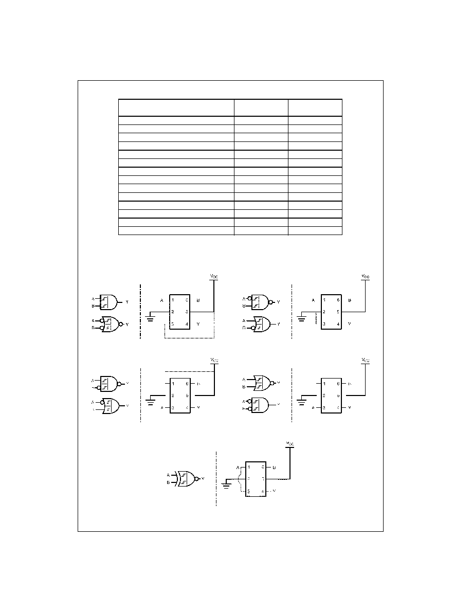
Logic Configurations NC7SZ57
Figure 1 through Figure 5 show the logical functions that can be implemented using the NC7SZ57. The diagrams show the
DeMorgan's equivalent logic duals for a given 2-input function. Next to the logical implementation is the board level physical
implementation of how the pins of the function should be connected.
FIGURE 1. 2-Input AND Gate
FIGURE 2. 2-Input NAND with Inverted A Input
FIGURE 3. 2-Input NAND with Inverted B Input
FIGURE 4. 2-Input NOR Gate
FIGURE 5. 2-Input XNOR Gate
2-Input Logic Function
Device Connection
Selection
Configuration
2-Input AND
NC7SZ57
Figure 1
2-Input AND with inverted input
NC7SZ58
Figures 7, 8
2-Input AND with both inputs inverted
NC7SZ57
Figure 4
2-Input NAND
NC7SZ58
Figure 6
2-Input NAND with inverted input
NC7SZ57
Figures 2, 3
2-Input NAND with both inputs inverted
NC7SZ58
Figure 9
2-Input OR
NC7SZ58
Figure 9
2-Input OR with inverted input
NC7SZ57
Figures 2, 3
2-Input OR with both inputs inverted
NC7SZ58
Figure 6
2-Input NOR
NC7SZ57
Figure 4
2-Input NOR with inverted input
NC7SZ58
Figures 7, 8
2-Input NOR with both inputs inverted
NC7SZ57
Figure 1
2-Input XOR
NC7SZ58
Figure 10
2-Input XNOR
NC7SZ57
Figure 5
www.fairchildsemi.com
4
NC7SZ57
∑
NC7SZ58
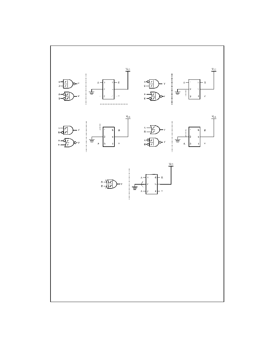
Logic Configurations NC7SZ58
Figure 6 through Figure 10 show the logical functions that can be implemented using the NC7SZ58. The diagrams show
the DeMorgan's equivalent logic duals for a given 2-input function. Next to the logical implementation is the board level
physical implementation of how the pins of the function should be connected.
FIGURE 6. 2-Input NAND Gate
FIGURE 7. 2-Input AND with Inverted A Input
FIGURE 8. 2-Input AND with Inverted B Input
FIGURE 9. 2-Input OR Gate
FIGURE 10. 2-Input XOR Gate

5
www.fairchildsemi.com
NC7SZ57
∑
NC
7
S
Z
5
8
Absolute Maximum Ratings
(Note 1)
Recommended Operating
Conditions
Note 1: Absolute maximum ratings are DC values beyond which the device
may be damaged or have its useful life impaired. The datasheet specifica-
tions should be met, without exception, to ensure that the system design is
reliable over its power supply, temperature, and output/input loading vari-
ables. Fairchild does not recommend operation outside datasheet specifi-
cations.
DC Electrical Characteristics
Supply Voltage (V
CC
)
-
0.5V to
+
7.0V
DC Input Voltage (V
IN
)
-
0.5V to
+
7.0V
DC Output Voltage (V
OUT
)
-
0.5V to
+
7.0V
DC Input Diode Current (I
IK
)
@ V
IN
0.5V
-
50 mA
DC Output Diode Current (I
OK
)
@ V
IN
-
0.5V
-
50 mA
DC Output Source/Sink Current (I
OUT
)
±
50 mA
DC V
CC
or Ground Current (I
CC
/ I
GND
)
±
50 mA
Storage Temperature Range (T
STG
)
-
65
∞
C to
+
150
∞
C
Max Junction Temperature under Bias (T
J
)
150
∞
C
Lead Temperature (T
L
)
(Soldering, 10 seconds)
260
∞
C
Power Dissipation (P
D
) @
+
85
∞
C
SC70-6
180 mW
Supply Voltage Operating (V
CC
)
1.65V to 5.5V
Supply Voltage Data Retention (V
CC
)
1.5V to 5.5V
Input Voltage (V
IN
)
0V to 5.5V
Output Voltage (V
OUT
)
0V to V
CC
Operating Temperature (T
A
)
-
40
∞
C to
+
85
∞
C
Thermal Resistance (
JA
)
SC70-6
350
∞
C/W
Symbol
Parameter
V
CC
T
A
=
+
25
∞
C
T
A
=
-
40
∞
C to
+
85
∞
C
Units
Conditions
(V)
Min
Typ
Max
Min
Max
V
P
Positive Threshold Voltage
1.65
0.6
0.99
1.4
0.6
1.4
V
2.3
1.0
1.39
1.8
1.0
1.8
3.0
1.3
1.77
2.2
1.3
2.2
4.5
1.9
2.49
3.1
1.9
3.1
5.5
2.2
2.95
3.6
2.2
3.6
V
N
Negative Threshold Voltage
1.65
0.2
0.50
0.9
0.2
0.9
V
2.3
0.4
0.75
1.15
0.4
1.15
3.0
0.6
0.99
1.5
0.6
1.5
4.5
1.0
1.43
2.0
1.0
2.0
5.5
1.2
1.70
2.3
1.2
2.3
V
H
Hysteresis Voltage
1.65
0.15
0.48
0.9
0.15
0.9
V
2.3
0.25
0.64
1.1
0.25
1.1
3.0
0.4
0.78
1.2
0.4
1.2
4.5
0.6
1.06
1.5
0.6
1.5
5.5
0.7
1.25
1.7
0.7
1.7
V
OH
HIGH Level Output Voltage
1.65
1.55
1.65
1.55
V
2.3
2.2
2.3
2.2
V
IN
=
V
IH
I
OH
=
-
100
µ
A
3.0
2.9
3.0
2.9
or V
IL
4.5
4.4
4.5
4.4
1.65
1.29
1.52
1.29
V
I
OH
=
-
4 mA
2.3
1.9
2.15
1.9
V
IN
=
V
IH
I
OH
=
-
8 mA
3.0
2.4
2.80
2.4
or V
IL
I
OH
=
-
16 mA
3.0
2.3
3.68
2.3
I
OH
=
-
24 mA
4.5
3.8
4.20
3.8
I
OH
=
-
32 mA
V
OL
LOW Level Output Voltage
1.65
0.0
0.10
0.10
V
2.3
0.0
0.10
0.10
V
IN
=
V
IH
I
OL
=
100
µ
A
3.0
0.0
0.10
0.10
or V
IL
4.5
0.0
0.10
0.10
1.65
0.08
0.24
0.24
V
I
OL
=
4 mA
2.3
0.10
0.3
0.3
V
IN
=
V
IH
I
OL
=
8 mA
3.0
0.15
0.4
0.4
or V
IL
I
OL
=
16 mA
3.0
0.22
0.55
0.55
I
OL
=
24 mA
4.5
0.22
0.55
0.55
I
OL
=
32 mA
I
IN
Input Leakage Current
0
-
5.5
±
0.1
±
1
µ
A
V
IN
=
5.5V, GND

www.fairchildsemi.com
6
NC7SZ57
∑
NC7SZ58
DC Electrical Characteristics
(Continued)
AC Electrical Characteristics
Note 2: C
PD
is defined as the value of the internal equivalent capacitance which is derived from dynamic operating current consumption (I
CCD
) at no output
loading and operating at 50% duty cycle. (See Figure 12) C
PD
is related to I
CCD
dynamic operatic current by the expression:
I
CCD
=
(C
PD
)(V
CC
)(f
in
)
+
(I
CC
static).
Symbol
Parameter
V
CC
T
A
=
+
25
∞
C
T
A
=
-
40
∞
C to
+
85
∞
C
Units
Conditions
(V)
Min
Typ
Max
Min
Max
I
OFF
Power Off Leakage Current
0.0
1
10
µ
A
V
IN
or V
OUT
=
5.5V
I
CC
Quiescent Supply Current
1.65
-
5.5
1
10
µ
A
V
IN
=
5.5V, GND
Symbol
Parameter
V
CC
T
A
=
+
25
∞
C
T
A
=
-
40
∞
C to
+
85
∞
C
Units
Conditions
Fig. No.
(V)
Min
Typ
Max
Min
Max
t
PLH
Propagation Delay I
n
to Y
1.8
±
0.15
3.0
8
14.0
3.0
14.5
ns
Figures
11, 13
t
PHL
2.5
±
0.2
1.5
4.9
8.0
1.5
8.5
C
L
=
15 pF
3.3
±
0.3
1.2
3.7
5.3
1.2
5.7
R
L
=
1 M
5.0
±
0.5
0.8
2.8
4.3
0.8
4.6
t
PLH
Propagation Delay I
n
to Y
3.3
±
0.3
1.5
4.2
6.0
1.5
6.5
ns
C
L
=
50pF
Figures
11, 13
t
PHL
5.0
±
0.5
1.0
3.4
4.9
1.0
5.3
R
L
=
500
C
IN
Input Capacitance
0
2
pF
C
PD
Power Dissipation
3.3
14
pF
(Note 2)
Figure 12
Capacitance
5.0
17

7
www.fairchildsemi.com
NC7SZ57
∑
NC
7
S
Z
5
8
AC Loading and Waveforms
C
L
includes load and stray Capacitance
Input PRR
=
1.0 MHz, t
W
=
500 ns
FIGURE 11. AC Test Circuit
Input
=
AC Waveforms
PRR
=
Variable; Duty Cycle
=
50%
FIGURE 12. I
CCD
Test Circuit
FIGURE 13. AC Waveforms

www.fairchildsemi.com
8
NC7SZ57
∑
NC7SZ58
Tape and Reel Specification
TAPE FORMAT for SC70
TAPE DIMENSIONS inches (millimeters)
Package
Tape
Number
Cavity
Cover Tape
Designator
Section
Cavities
Status
Status
Leader (Start End)
125 (typ)
Empty
Sealed
P6X
Carrier
3000
Filled
Sealed
Trailer (Hub End)
75 (typ)
Empty
Sealed
Package
Tape Size
DIM A
DIM B
DIM F
DIM K
o
DIM P1
DIM W
SC70-6
8 mm
0.093
0.096
0.138
±
0.004 0.053
±
0.004
0.157
0.315
±
0.004
(2.35)
(2.45)
(3.5
±
0.10)
(1.35
±
0.10)
(4)
(8
±
0.1)

9
www.fairchildsemi.com
NC7SZ57
∑
NC
7
S
Z
5
8
Tape and Reel Specification
(Continued)
TAPE FORMAT for MicroPak
REEL DIMENSIONS inches (millimeters)
Package
Tape
Number
Cavity
Cover Tape
Designator
Section
Cavities
Status
Status
Leader (Start End)
125 (typ)
Empty
Sealed
L6X
Carrier
3000
Filled
Sealed
Trailer (Hub End)
75 (typ)
Empty
Sealed
Tape
Size
A
B
C
D
N
W1
W2
W3
8 mm
7.0
0.059
0.512
0.795
2.165
0.331
+
0.059/
-
0.000
0.567
W1
+
0.078/
-
0.039
(177.8)
(1.50)
(13.00)
(20.20)
(55.00)
(8.40
+
1.50/
-
0.00)
(14.40)
(W1
+
2.00/
-
1.00)

www.fairchildsemi.com
10
NC7SZ57
∑
NC7SZ58
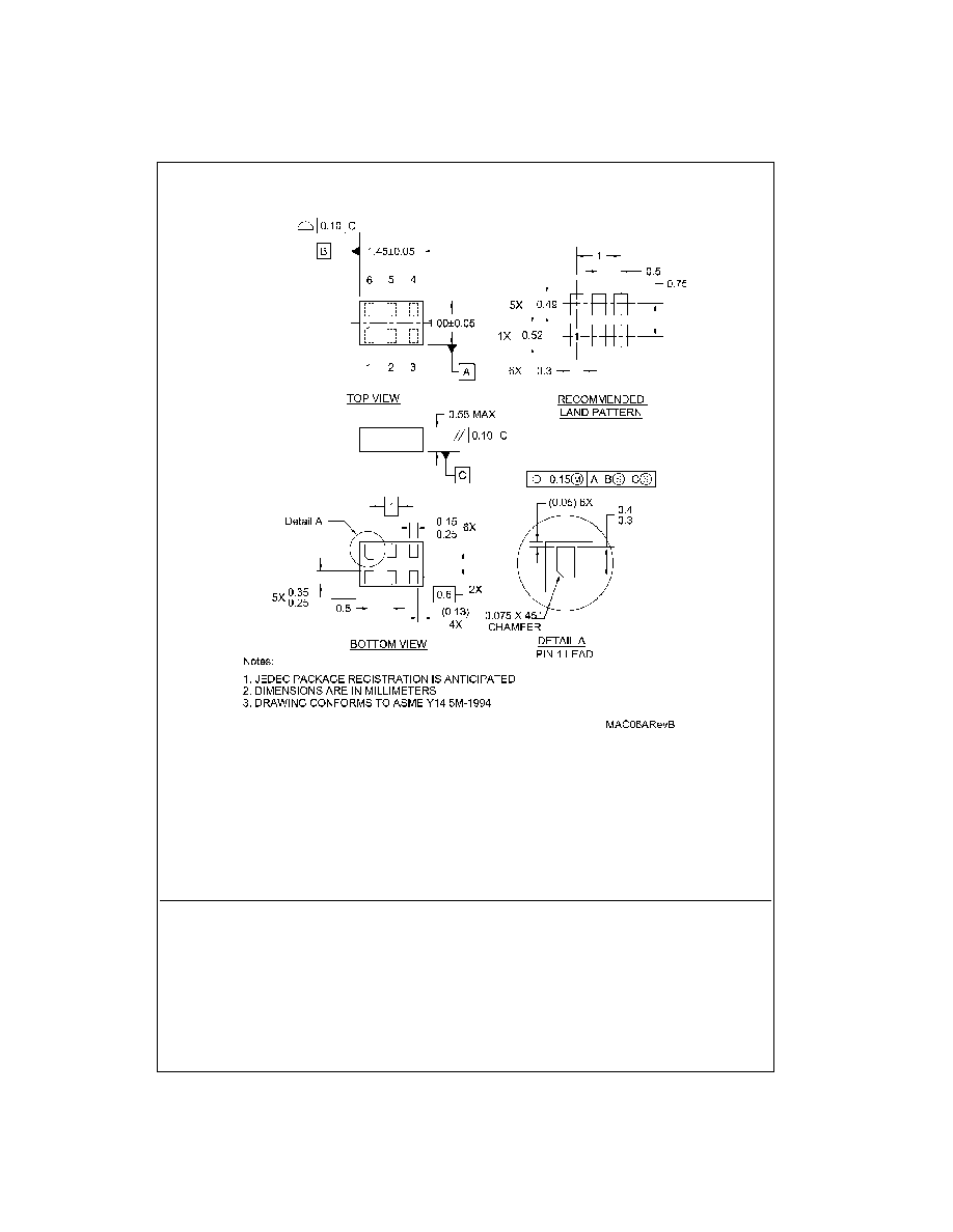
Physical Dimensions
inches (millimeters) unless otherwise noted
6-Lead SC70, EIAJ SC88, 1.25mm Wide
Package Number MAA06A
11
www.fairchildsemi.com
NC7SZ57
∑
N
C
7SZ5
8
T
i
ny
Logic
UH
S Unive
r
sal
Conf
igur
abl
e
2-
Input
Logic Gates
Physical Dimensions
inches (millimeters) unless otherwise noted (Continued)
6-Lead MicroPak, 1.0mm Wide
Package Number MAC06A
Fairchild does not assume any responsibility for use of any circuitry described, no circuit patent licenses are implied and
Fairchild reserves the right at any time without notice to change said circuitry and specifications.
LIFE SUPPORT POLICY
FAIRCHILD'S PRODUCTS ARE NOT AUTHORIZED FOR USE AS CRITICAL COMPONENTS IN LIFE SUPPORT
DEVICES OR SYSTEMS WITHOUT THE EXPRESS WRITTEN APPROVAL OF THE PRESIDENT OF FAIRCHILD
SEMICONDUCTOR CORPORATION. As used herein:
1. Life support devices or systems are devices or systems
which, (a) are intended for surgical implant into the
body, or (b) support or sustain life, and (c) whose failure
to perform when properly used in accordance with
instructions for use provided in the labeling, can be rea-
sonably expected to result in a significant injury to the
user.
2. A critical component in any component of a life support
device or system whose failure to perform can be rea-
sonably expected to cause the failure of the life support
device or system, or to affect its safety or effectiveness.
www.fairchildsemi.com