 | –≠–ª–µ–∫—Ç—Ä–æ–Ω–Ω—ã–π –∫–æ–º–ø–æ–Ω–µ–Ω—Ç: NC7SZ66 | –°–∫–∞—á–∞—Ç—å:  PDF PDF  ZIP ZIP |
© 2003 Fairchild Semiconductor Corporation
DS012177
www.fairchildsemi.com
November 1996
Revised August 2003
NC7SZ66
T
i
nyL
ogic
L
o
w
V
o
lt
age U
H
S Singl
e SP
ST Normal
ly Open
Bus Swit
ch
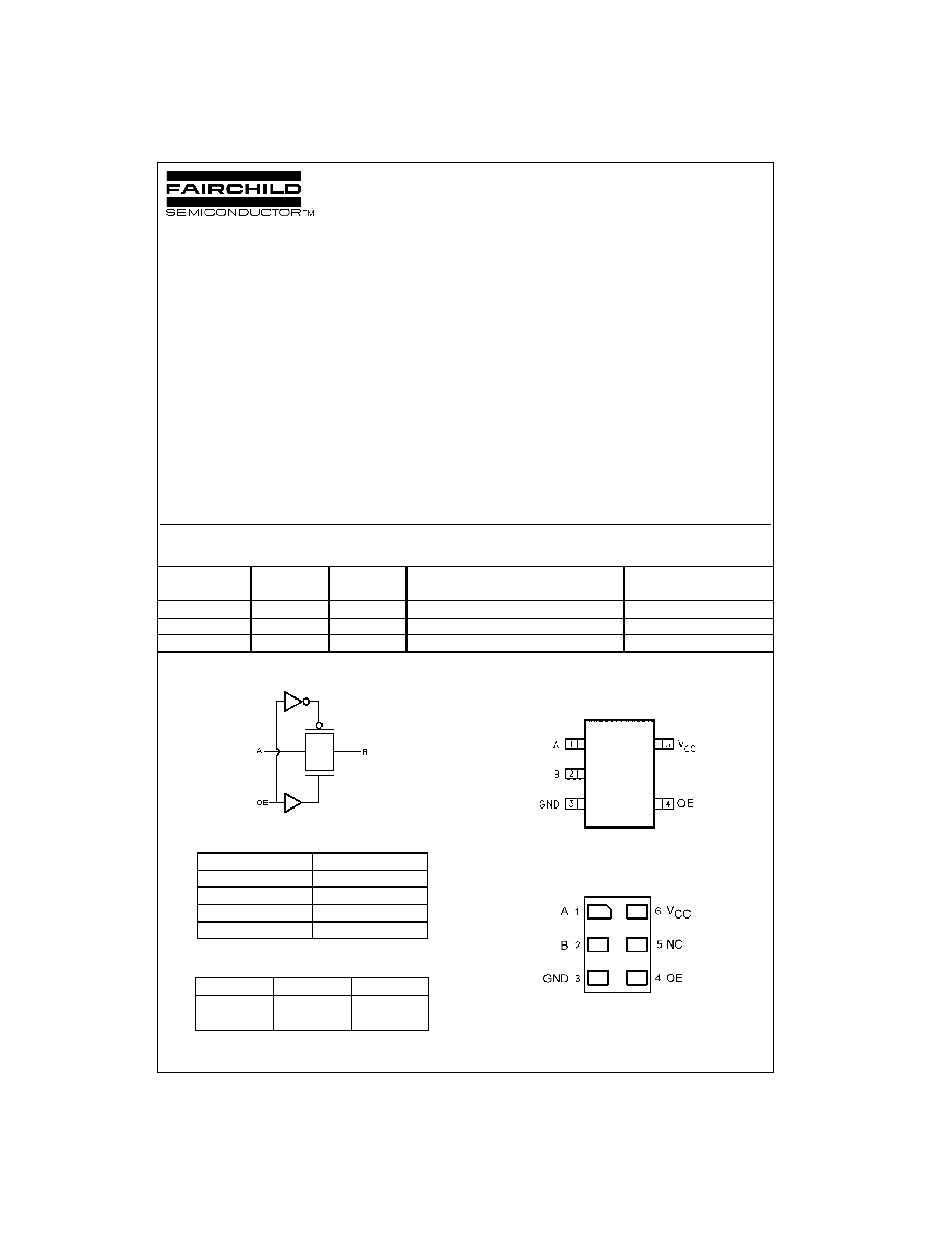
NC7SZ66
TinyLogic
Low Voltage UHS Single SPST
Normally Open Bus Switch
General Description
The NC7SZ66 is a ultra high-speed (UHS) CMOS compati-
ble single-pole/single-throw (SPST) bus switch. The LOW
On Resistance of the switch allows inputs to be connected
to outputs with minimal propagation delay and without gen-
erating additional ground bounce noise. The device is
organized as a 1-bit switch with a switch enable (OE) sig-
nal. When OE is HIGH, the switch is on and Port A is con-
nected to Port B. When OE is LOW, the switch is open and
a high-impedance state exists between the two ports.
Features
s
Space saving SOT23 or SC70 5-lead package
s
Ultra small MicroPak
leadless package
s
Broad V
CC
Operating Range 1.65V≠5.5V
s
Rail-to-rail signal handling
s
5
switch connection between two ports
s
Minimal propagation delay through the switch
s
Low I
CC
s
Zero bounce in flow-through mode
s
Control input compatible with CMOS input levels
Ordering Code:
Logic Symbol
Pin Descriptions
Function Table
Connection Diagrams
Pin Assignments for SC70
(Top View)
Pad Assignment for MicroPak
(Top Through View)
TinyLogic
is a registered trademark of Fairchild Semiconductor Corporation.
MicroPak
is a trademark of Fairchild Semiconductor Corporation.
Order
Package Product
Code
Package Description
Supplied As
Number
Number
Top Mark
NC7SZ66M5X
MA05B
7Z66
5-Lead SOT23, JEDEC MO-178, 1.6mm
3k Units on Tape and Reel
NC7SZ66P5X
MAA05A
Z66
5-Lead SC70, EIAJ SC-88a, 1.25mm Wide
3k Units on Tape and Reel
NC7SZ66L6X
MAC06
EE
6-Lead MicroPak, 1.0mm Wide
5k Units on Tape and Reel
Pin Names
Description
OE
Switch Enable Input
A
Bus A I/O
B
Bus B I/O
NC
No Connect
OE
B
0
Function
L
HIGH-Z State
Disconnect
H
A
0
Connect
www.fairchildsemi.com
2
NC7SZ66
Absolute Maximum Ratings
(Note 1)
Recommended Operating
Conditions
(Note 3)
Note 1: The "Absolute Maximum Ratings" are those values beyond which
the safety of the device cannot be guaranteed. The device should not be
operated at these limits. The parametric values defined in the Electrical
Characteristics tables are not guaranteed at the absolute maximum ratings.
The "Recommended Operating Conditions" table will define the conditions
for actual device operation.
Note 2: The input and output negative voltage ratings may be exceeded if
the input and output diode current ratings are observed.
Note 3: Unused inputs must be held HIGH or LOW. They may not float.
DC Electrical Characteristics
Note 4: Measured by the voltage drop between A and B pins at the indicated current through the switch. On Resistance is determined by the lower of the
voltages on the two (A or B) pins.
Note 5: All typical values are at the specified V
CC
, and T
A
=
25
∞
C.
Note 6: Parameter is characterized but not tested in production.
Note 7: Flatness is defined as the difference between the maximum and minimum value of On Resistance over the specified range of conditions.
Supply Voltage (V
CC
)
-
0.5V to
+
7.0V
DC Switch Voltage (V
S
)
-
0.5V to V
CC
+
0.5V
DC Input Voltage (V
IN
) (Note 2)
-
0.5V to
+
7.0V
DC Input Diode Current
(I
IK
) V
IN
<
0V
-
50 mA
DC Output (I
OUT
) Sink Current
128 mA
DC V
CC
/GND Current (I
CC
/I
GND
)
±
100 mA
Storage Temperature Range
(T
STG
)
-
65
∞
C to
+
150
∞
C
Junction Lead Temperature
under Bias (T
J
)
+
150
∞
C
Junction Lead Temperature (T
L
)
(Soldering, 10 Seconds)
+
260
∞
C
Power Dissipation (P
D
) @
+
85
∞
C
SOT23-5
200 mW
SC70-5
150 mW
Power Supply Operating (V
CC
)
1.65V to 5.5V
Control Input Voltage (V
IN
)
0V to 5.5V
Switch Input Voltage (V
IN
)
0V to V
CC
Switch Output Voltage (V
OUT
)
0V to V
CC
Input Rise and Fall Time (t
r
, t
f
)
Control Input; V
CC
=
2.3V
-
3.6V
0 ns/V to 10 ns
Control Input; V
CC
=
4.5
-
5.5V
0 ns/V to 5 ns
Switch I/O
0 ns/V to DC
Operating Temperature (T
A
)
-
40
∞
C to
+
85
∞
C
Thermal Resistance (
JA
)
SOT23-5
300
∞
C/Watt
SC70-5
425
∞
C/Watt
Symbol
Parameter
V
CC
T
A
=
-
40
∞
C to
+
85
∞
C
T
A
=
+
25
∞
C
Units
Conditions
(V)
Min
Typ
(Note 5)
Max
Min
Typ
Max
V
IH
HIGH Level
1.65 to 1.95 0.75 V
CC
V
Input Voltage
2.3 to 5.5
0.7 V
CC
V
IL
LOW Level
1.65 to 1.95
0.25 V
CC
V
Input Voltage
2.3 to 5.5
0.3 V
CC
I
IN
Control Input
0 to 5.5
±
0.05
±
1.0
µ
A
0
V
IN
5.5V
Leakage Current
I
OFF
OFF Leakage Current
1.65 to 5.5
±
0.05
±
10.0
µ
A
0
A, B
V
CC
R
ON
Switch On Resistance
4.5
3
7
V
IN
=
0V, I
IN
=
30 mA
(Note 4)
5
12
V
IN
=
2.4V, I
IN
=
15 mA
7
15
V
IN
=
4.5V, I
IN
=
30 mA
3.0
4
9
V
IN
=
0V, I
IN
=
24 mA
10
20
V
IN
=
3V, I
IN
=
24 mA
2.3
5
12
V
IN
=
0V, I
IN
=
8 mA
13
30
V
IN
=
2.3V, I
IN
=
8 mA
1.8
7
28
V
IN
=
0V, I
IN
=
4 mA
25
60
V
IN
=
1.8V, I
IN
=
4 mA
R
flat
On Resistance Flatness
5.0
6
I
A
=
-
30 mA, 0
V
Bn
V
CC
(Note 4)(Note 6)(Note 7)
3.3
12
I
A
=
-
24 mA, 0
V
Bn
V
CC
2.5
28
I
A
=
-
8 mA, 0
V
Bn
V
CC
1.8
125
I
A
=
-
4 mA, 0
V
Bn
V
CC
I
CC
Quiescent Supply Current
1.65 to 5.5
0.05
10
µ
A
V
IN
=
V
CC
or GND
I
OUT
=
0
3
www.fairchildsemi.com
NC7SZ66
AC Electrical Characteristics
Note 8: All typical values are at the specified V
CC
, and T
A
=
25
∞
C.
Note 9: This parameter is guaranteed by design but is not tested. The switch contributes no propagation delay other than the RC delay of the typical On
Resistance of the switch and the 50 pF load capacitance, when driven by an ideal voltage source (zero output impedance).
Capacitance
T
A
=
-
40
∞
C to
+
85
∞
C,
Symbol
Parameter
V
CC
C
L
=
50 pF, RU
=
RD
=
500
Units
Conditions
Figure
(V)
Min
Typ
(Note 8)
Max
Number
t
PHL
, t
PLH
Propagation Delay Bus to Bus
1.65 to 1.95
4.3
Figures
1, 2
(Note 9)
2.3-2.7
1.2
ns
V
IN
=
OPEN
3.0-3.6
0.8
ns
4.5-5.5
0.3
ns
t
PZL
, t
PZH
Output Enable Time
1.65 to 1.95
1.5
7.0
14.2
Figures
1, 2
2.3-2.7
1.5
3.3
7.0
ns
V
IN
=
2 x V
CC
for t
PZL
3.0-3.6
1.5
2.4
5.5
ns
V
IN
=
0V for t
PZH
4.5-5.5
1.5
2.0
4.5
ns
t
PLZ
, t
PHZ
Output Disable Time
1.65 to 1.95
1.5
9.2
18.2
Figures
1, 2
2.3-2.7
1.5
5.3
9.0
ns
V
IN
=
2 x V
CC
for t
PLZ
3.0-3.6
1.5
4.0
7.0
ns
V
IN
=
0V for t
PHZ
4.5-5.5
1.5
2.7
5.0
ns
Symbol Parameter
Typ
Max
Units
Conditions
C
IN
Control Pin Input Capacitance
2
pF
V
CC
=
0V
C
I/O
Input/Output Capacitance
6
pF
V
CC
=
5.0V

www.fairchildsemi.com
4
NC7SZ66
AC Loading and Waveforms
Input driven by 50
source terminated in 50
C
L
includes load and stray capacitance.
Input PRR
=
1.0 MHz; t
w
=
500 ns
FIGURE 1. AC Test Circuit
FIGURE 2. AC Waveforms
5
www.fairchildsemi.com
NC7SZ66
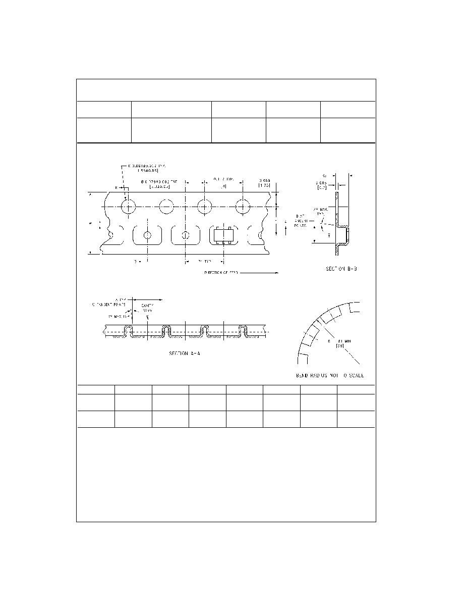
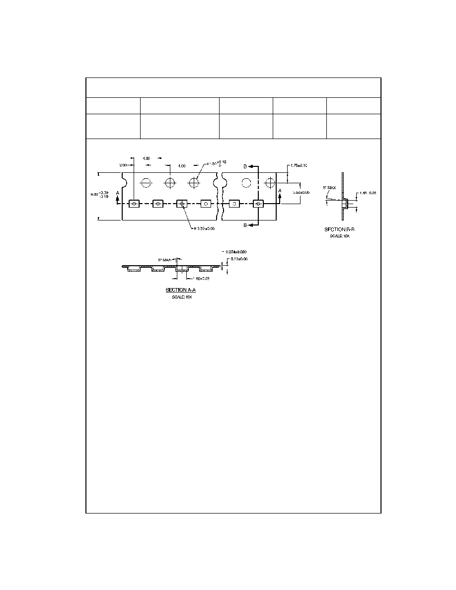
Tape and Reel Specification
TAPE FORMAT FOR SOT23, SC70
TAPE DIMENSIONS inches (millimeters)
Package
Tape
Number
Cavity
Cover Tape
Designator
Section
Cavities
Status
Status
Leader (Start End)
125 (typ)
Empty
Sealed
M5X, P5X
Carrier
3000
Filled
Sealed
Trailer (Hub End)
75 (typ)
Empty
Sealed
Package
Tape Size
DIM A
DIM B
DIM F
DIM K
o
DIM P1
DIM W
SC70-5
8 mm
0.093
0.096
0.138
±
0.004 0.053
±
0.004
0.157
0.315
±
0.004
(2.35)
(2.45)
(3.5
±
0.10)
(1.35
±
0.10)
(4)
(8
±
0.1)
SOT23-5
8 mm
0.130
0.130
0.138
±
0.002 0.055
±
0.004
0.157
0.315
±
0.012
(3.3)
(3.3)
(3.5
±
0.05)
(1.4
±
0.11)
(4)
(8
±
0.3)
www.fairchildsemi.com
6
NC7SZ66
Tape and Reel Specification
(Continued)
TAPE FORMAT FOR MicroPak
TAPE DIMENSIONS inches (millimeters)
Package
Tape
Number
Cavity
Cover Tape
Designator
Section
Cavities
Status
Status
Leader (Start End)
125 (typ)
Empty
Sealed
L6X
Carrier
5000
Filled
Sealed
Trailer (Hub End)
75 (typ)
Empty
Sealed
7
www.fairchildsemi.com
NC7SZ66
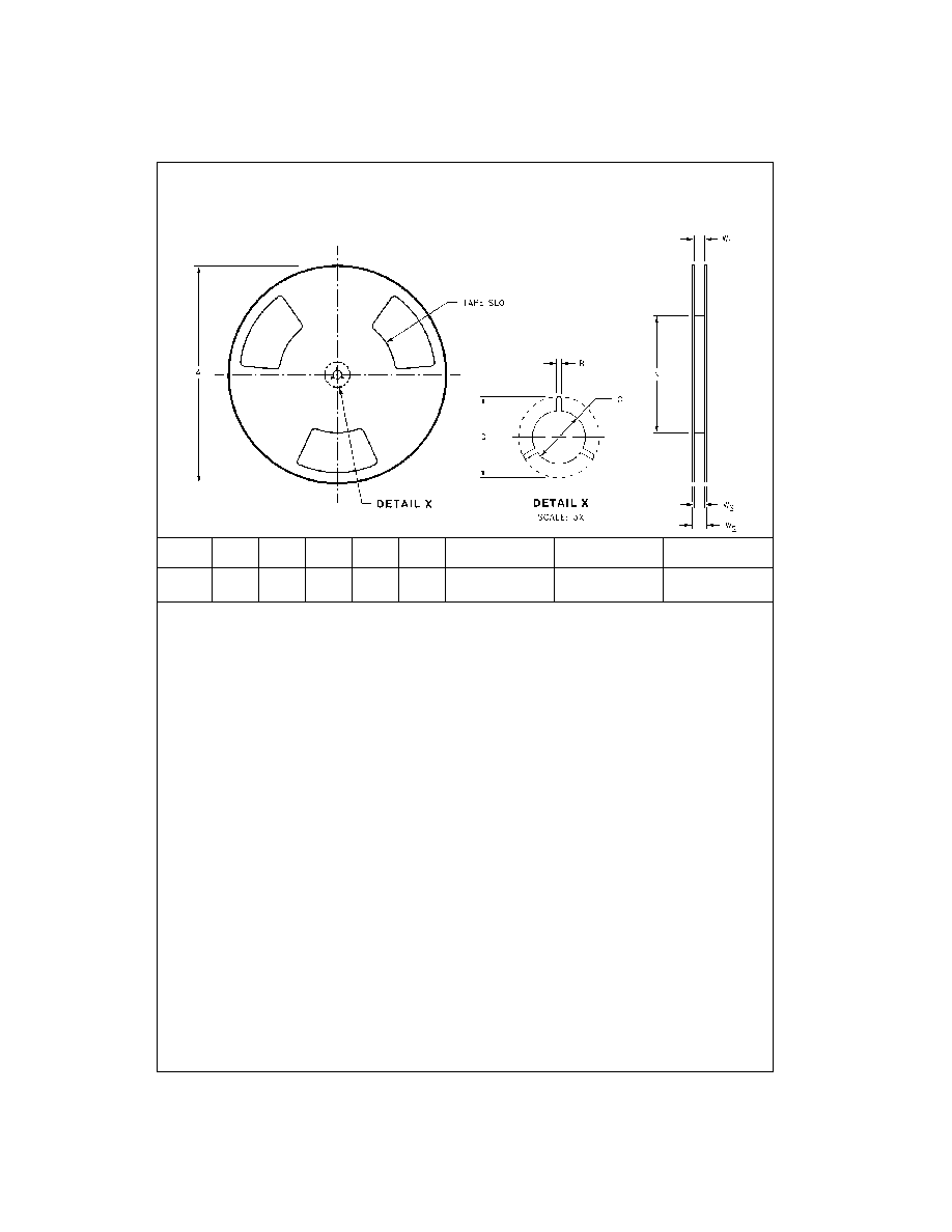
Tape and Reel Specification
(Continued)
REEL DIMENSIONS inches (millimeters)
Tape
Size
A
B
C
D
N
W1
W2
W3
8 mm
7.0
0.059
0.512
0.795
2.165
0.331
+
0.059/
-
0.000
0.567
W1
+
0.078/
-
0.039
(177.8)
(1.50)
(13.00)
(20.20)
(55.00)
(8.40
+
1.50/
-
0.00)
(14.40)
(W1
+
2.00/
-
1.00)
www.fairchildsemi.com
8
NC7SZ66
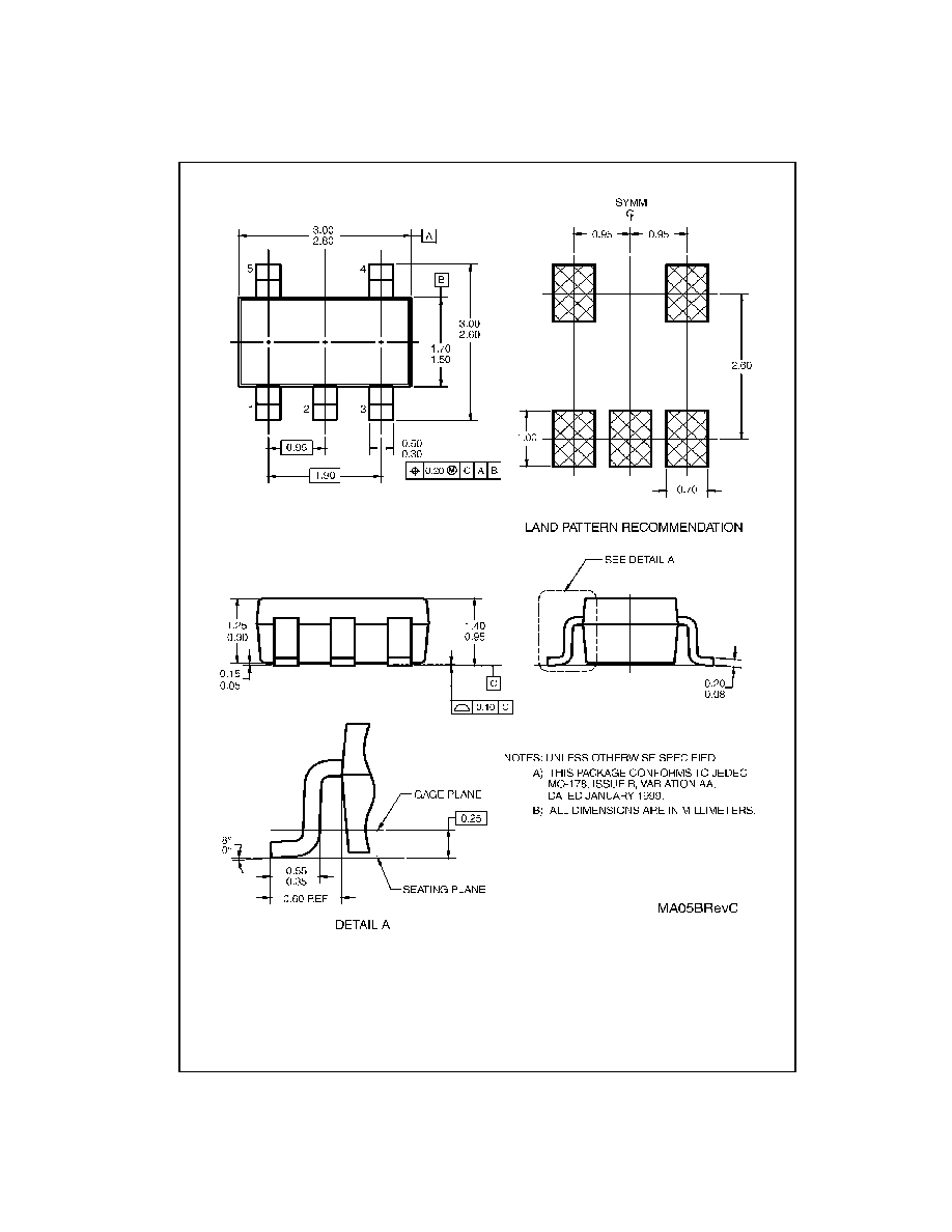
Physical Dimensions
inches (millimeters) unless otherwise noted
5-Lead SOT23, JEDEC MO-178, 1.6mm
Package Number MA05B
9
www.fairchildsemi.com
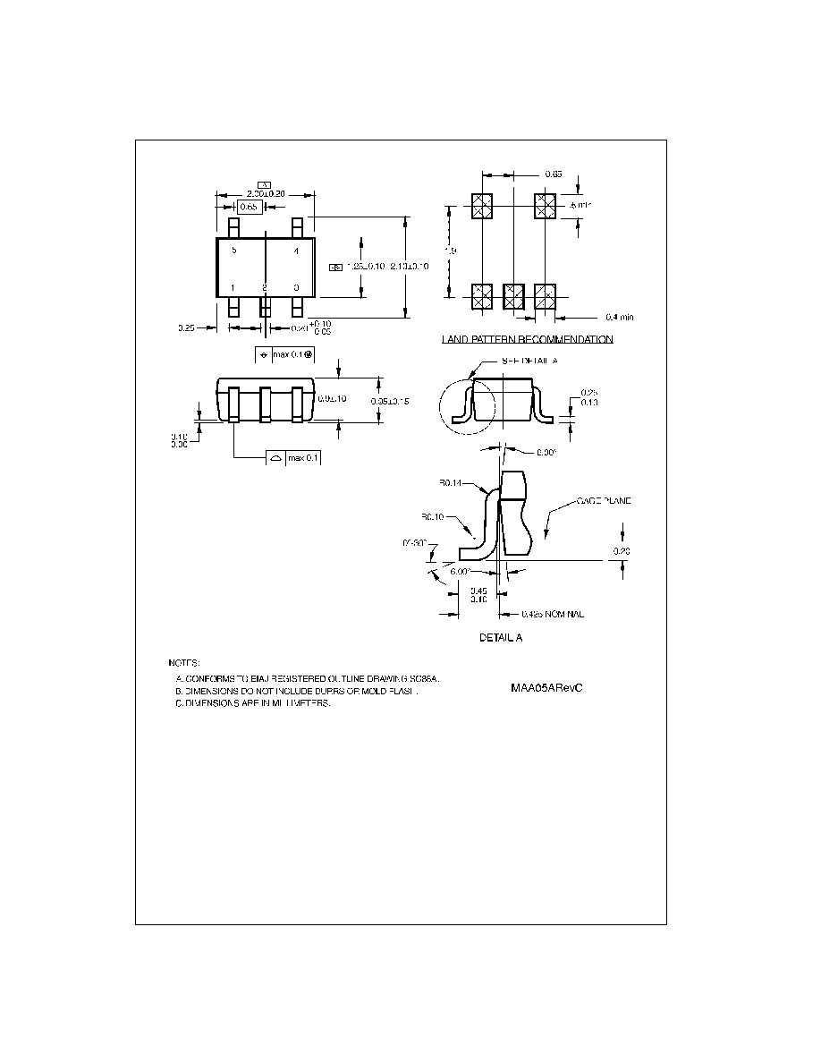
NC7SZ66
Physical Dimensions
inches (millimeters) unless otherwise noted (Continued)
5-Lead SC70, EIAJ SC-88a, 1.25mm Wide
Package Number MAA05A
www.fairchildsemi.com
10
NC7SZ66 T
i
nyLogi
c
Low V
o
l
t
a
ge
UHS S
i
ngl
e
SPST Normall
y
O
pen
Bus Sw
i
t
c
h
Physical Dimensions
inches (millimeters) unless otherwise noted (Continued)
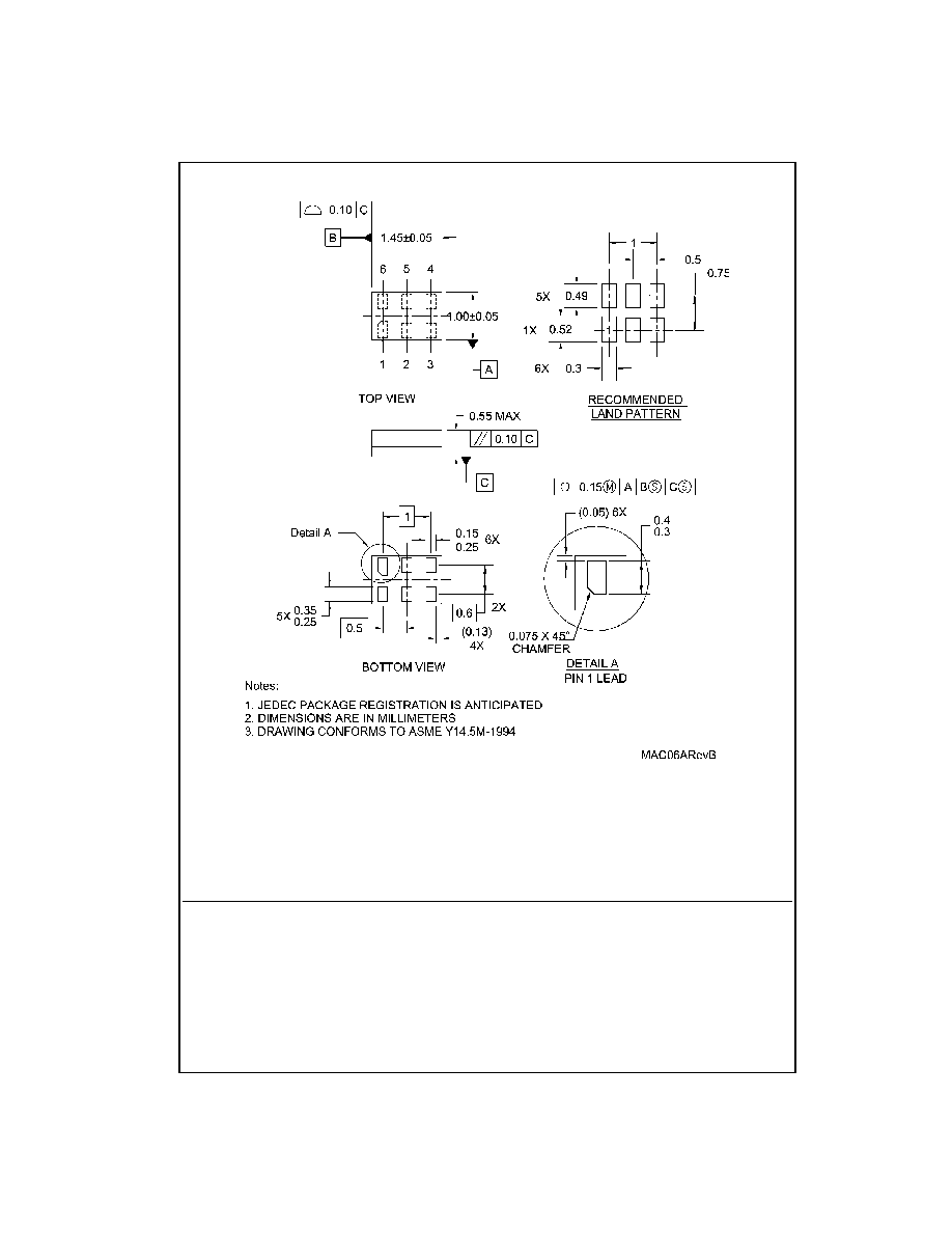
6-Lead MicroPak, 1.0mm Wide
Package Number MAC06A
Fairchild does not assume any responsibility for use of any circuitry described, no circuit patent licenses are implied and
Fairchild reserves the right at any time without notice to change said circuitry and specifications.
LIFE SUPPORT POLICY
FAIRCHILD'S PRODUCTS ARE NOT AUTHORIZED FOR USE AS CRITICAL COMPONENTS IN LIFE SUPPORT
DEVICES OR SYSTEMS WITHOUT THE EXPRESS WRITTEN APPROVAL OF THE PRESIDENT OF FAIRCHILD
SEMICONDUCTOR CORPORATION. As used herein:
1. Life support devices or systems are devices or systems
which, (a) are intended for surgical implant into the
body, or (b) support or sustain life, and (c) whose failure
to perform when properly used in accordance with
instructions for use provided in the labeling, can be rea-
sonably expected to result in a significant injury to the
user.
2. A critical component in any component of a life support
device or system whose failure to perform can be rea-
sonably expected to cause the failure of the life support
device or system, or to affect its safety or effectiveness.
www.fairchildsemi.com