 | –≠–ª–µ–∫—Ç—Ä–æ–Ω–Ω—ã–π –∫–æ–º–ø–æ–Ω–µ–Ω—Ç: NC7WP86 | –°–∫–∞—á–∞—Ç—å:  PDF PDF  ZIP ZIP |

© 2005 Fairchild Semiconductor Corporation
DS500814
www.fairchildsemi.com
June 2003
Revised January 2005
NC7WP86 T
i
nyLogi
c
ULP
Dual
2-I
nput Excl
usive
OR
Gat
e
NC7WP86
TinyLogic
ULP Dual 2-Input Exclusive OR Gate
General Description
The NC7WP86 is a dual 2-input Exclusive OR Gate from
Fairchild's Ultra Low Power (ULP) series of TinyLogic
.
Ideal for applications where battery life is critical, this prod-
uct is designed for ultra low power consumption within the
V
CC
operating range of 0.9V to 3.6V V
CC
.
The internal circuit is composed of a minimum of inverter
stages, including the output buffer, to enable ultra low static
and dynamic power.
The NC7WP86 is designed for optimized power and
speed, and is fabricated with an advanced CMOS technol-
ogy to achieve high speed operation while maintaining
extremely low CMOS power dissipation.
Features
s
Space saving US8 package
s
Ultra small MicroPak
Pb-Free package
s
0.9V to 3.6V V
CC
supply operation
s
3.6V overvoltage tolerant I/O's at V
CC
from 0.9V to 3.6V
s
t
PD
3.0 ns typ for 3.0V to 3.6V V
CC
4.0 ns typ for 2.3V to 2.7V V
CC
5.0 ns typ for 1.65V to 1.95V V
CC
6.0 ns typ for 1.40V to 1.60V V
CC
9.0 ns typ for 1.10V to 1.30V V
CC
26.0 ns typ for 0.90V V
CC
s
Power-Off high impedance inputs and outputs
s
Static Drive (I
OH
/I
OL
)
±
2.6 mA @ 3.00V V
CC
±
2.1 mA @ 2.30V V
CC
±
1.5 mA @ 1.65V V
CC
±
1.0 mA @ 1.40V V
CC
±
0.5 mA @ 1.10V V
CC
±
20
µ
A @ 0.9V V
CC
s
Low noise switching using design techniques of
Quiet Series
noise/EMI reduction circuitry
s
Ultra Low dynamic power
Ordering Code:
Pb-Free package per JEDEC J-STD-020B.
Battery Life vs. V
CC
Supply Voltage
TinyLogic ULP and ULP-A with up to 50% less power consumption can
extend your battery life significantly.
Battery Life
=
(V
battery
*I
battery
*.9)/(P
device
)/24hrs/day
Where, P
device
=
(I
CC
* V
CC
)
+
(C
PD
+
C
L
) * V
CC
2
* f
Assumes ideal 3.6V Lithium Ion battery with current rating of 900mAH and
derated 90% and device frequency at 10MHz, with C
L
=
15 pF load
TinyLogic
is a registered trademark of Fairchild Semiconductor Corporation.
MicroPak
and Quiet Series
are trademarks of Fairchild Semiconductor Corporation.
Order Number
Product
Package Description
Supplied As
Package
Code
Number
Top Mark
NC7WP86K8X
MAB08A
WP86
8-Lead US8, JEDEC MO-187, Variation CA 3.1mm Wide 3k Units on Tape and Reel
NC7WP86L8X
MAC08A
Y7
Pb-Free 8-Lead MicroPak, 1.6 mm Wide
5k Units on Tape and Reel
www.fairchildsemi.com
2
NC7W
P
86
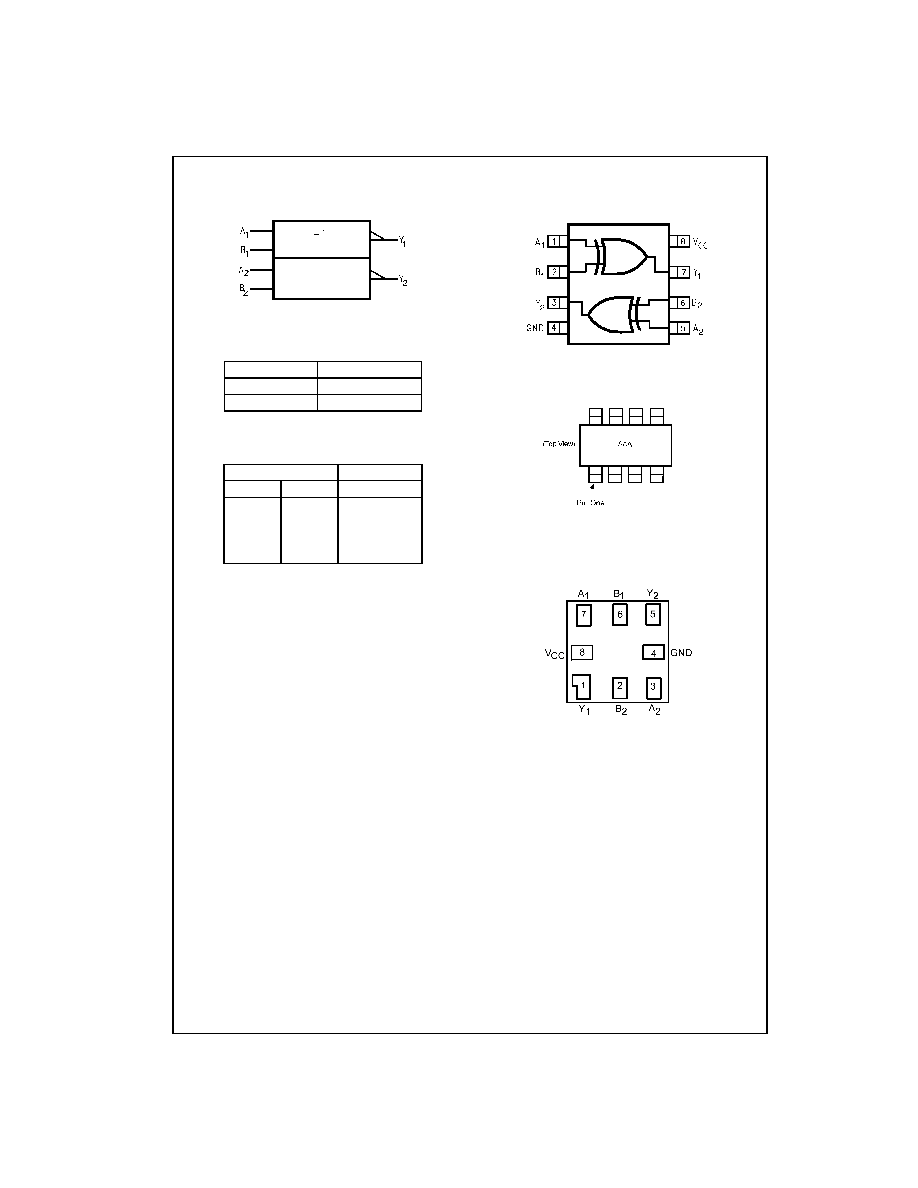
Logic Symbol
IEEE/IEC
Pin Descriptions
Function Table
Y
=
A
B
H
=
HIGH Logic Level
L
=
LOW Logic Level
Connection Diagrams
Pin Assignments for US8
(Top View)
Pin One Orientation Diagram
AAA represents Product Code Top Mark - see ordering code
Note: Orientation of Top Mark determines Pin One location. Read the top
product code mark left to right, Pin One is the lower left pin (see diagram).
Pad Assignments for MicroPak
(Top Thru View)
Pin Names
Description
A
n
, B
n
Input
Y
n
Output
Inputs
Output
A
B
Y
L
L
L
L
H
H
H
L
H
H
H
L
3
www.fairchildsemi.com
NC7WP86
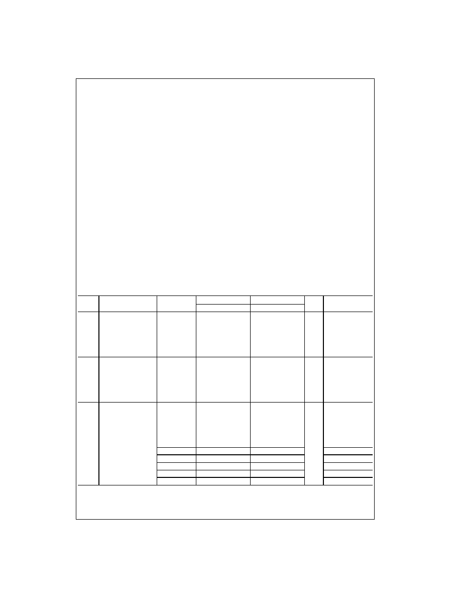
Absolute Maximum Ratings
(Note 1)
Recommended Operating
Conditions
(Note 3)
Note 1: Absolute Maximum Ratings: are those values beyond which the
safety of the device cannot be guaranteed. The device should not be oper-
ated at these limits. The parametric values defined in the Electrical Charac-
teristics tables are not guaranteed at the absolute maximum ratings. The
"Recommended Operating Conditions" table will define the conditions for
actual device operation.
Note 2: I
O
Absolute Maximum Rating must be observed.
Note 3: Unused inputs must be held HIGH or LOW. They may not float.
DC Electrical Characteristics
Supply Voltage (V
CC
)
-
0.5V to
+
4.6V
DC Input Voltage (V
IN
)
-
0.5V to
+
4.6V
DC Output Voltage (V
OUT
)
HIGH or LOW State (Note 2)
-
0.5V to V
CC
+
0.5V
V
CC
=
0V
-
0.5V to 4.6V
DC Input Diode Current (I
IK
) V
IN
<
0V
±
50 mA
DC Output Diode Current (I
OK
)
V
OUT
<
0V
-
50 mA
V
OUT
>
V
CC
+
50 mA
DC Output Source/Sink Current (I
OH
/I
OL
)
±
50 mA
DC V
CC
or Ground Current per
Supply Pin (I
CC
or Ground)
±
50 mA
Storage Temperature Range (T
STG
)
-
65
∞
C to
+
150
∞
C
Supply Voltage
0.9V to 3.6V
Input Voltage (V
IN
)
0V to 3.6V
Output Voltage (V
OUT
)
HIGH or LOW State
0V to V
CC
V
CC
=
0V
0V to 3.6V
Output Current in I
OH
/I
OL
V
CC
=
3.0V to 3.6V
±
2.6 mA
V
CC
=
2.3V to 2.7V
±
2.1 mA
V
CC
=
1.65V to 1.95V
±
1.5 mA
V
CC
=
1.40V to 1.60V
±
1.0 mA
V
CC
=
1.10V to 1.30V
±
0.5 mA
V
CC
=
0.9V
±
20
µ
A
Free Air Operating Temperature (T
A
)
-
40
∞
C to
+
85
∞
C
Minimum Input Edge Rate (
t/
V)
V
IN
=
0.8V to 2.0V, V
CC
=
3.0V
10 ns/V
Symbol
Parameter
V
CC
T
A
=
+
25
∞
C
T
A
=
-
40
∞
C to
+
85
∞
C
Units
Conditions
(V)
Min
Max
Min
Max
V
IH
HIGH Level
0.90
0.65 x V
CC
0.65 x V
CC
V
Input Voltage
1.10
V
CC
1.30
0.65 x V
CC
0.65 x V
CC
1.40
V
CC
1.60
0.65 x V
CC
0.65 x V
CC
1.65
V
CC
1.95
0.65 x V
CC
0.65 x V
CC
2.30
V
CC
2.70
1.6
1.6
3.00
V
CC
3.60
2.1
2.1
V
IL
LOW Level
0.90
0.35 x V
CC
0.35 x V
CC
V
Input Voltage
1.10
V
CC
1.30
0.35 x V
CC
0.35 x V
CC
1.40
V
CC
1.60
0.35 x V
CC
0.35 x V
CC
1.65
V
CC
1.95
0.35 x V
CC
0.35 x V
CC
2.30
V
CC
2.70
0.7
0.7
3.00
V
CC
3.60
0.9
0.9
V
OH
HIGH Level
0.90
V
CC
-
0.1
V
CC
-
0.1
V
I
OH
=
-
20
µ
A
Output Voltage
1.10
V
CC
1.30
V
CC
-
0.1
V
CC
-
0.1
1.40
V
CC
1.60
V
CC
-
0.1
V
CC
-
0.1
1.65
V
CC
1.95
V
CC
-
0.1
V
CC
-
0.1
2.30
V
CC
2.70
V
CC
-
0.1
V
CC
-
0.1
3.00
V
CC
3.60
V
CC
-
0.1
V
CC
-
0.1
1.10
V
CC
1.30
0.75 x V
CC
0.70 x V
CC
I
OH
=
-
0.5 mA
1.40
V
CC
1.60
1.07
0.99
I
OH
=
-
1.0 mA
1.65
V
CC
1.95
1.24
1.22
I
OH
=
-
1.5 mA
2.30
V
CC
2.70
1.95
1.87
I
OH
=
-
2.1 mA
3.00
V
CC
3.60
2.61
2.55
I
OH
=
-
2.6 mA
www.fairchildsemi.com
4
NC7W
P
86
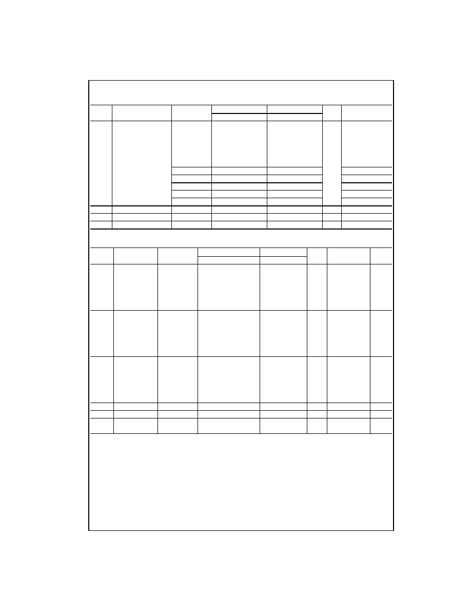
DC Electrical Characteristics
(Continued)
AC Electrical Characteristics
Symbol
Parameter
V
CC
T
A
=
+
25
∞
C
T
A
=
-
40
∞
C to
+
85
∞
C
Units
Conditions
(V)
Min
Max
Min
Max
V
OL
LOW Level
0.90
0.1
0.1
V
I
OL
=
20
µ
A
Output Voltage
1.10
V
CC
1.30
0.1
0.1
1.40
V
CC
1.60
0.1
0.1
1.65
V
CC
1.95
0.1
0.1
2.30
V
CC
2.70
0.1
0.1
3.00
V
CC
3.60
0.1
0.1
1.10
V
CC
1.30
0.30 x V
CC
0.30 x V
CC
I
OL
=
0.5 mA
1.40
V
CC
1.60
0.31
0.37
I
OL
=
1.0 mA
1.65
V
CC
1.95
0.31
0.35
I
OL
=
1.5 mA
2.30
V
CC
2.70
0.31
0.33
I
OL
=
2.1 mA
3.00
V
CC
3.60
0.31
0.33
I
OL
=
2.6 mA
I
IN
Input Leakage Current
0.90 to 3.60
±
0.1
±
0.5
µ
A
0
V
I
3.6V
I
OFF
Power Off Leakage Current
0
0.5
0.5
µ
A
0
(V
I
, V
O
)
3.6V
I
CC
Quiescent Supply Current
0.90 to 3.60
0.9
0.9
µ
A
V
I
=
V
CC
or GND
Symbol
Parameter
V
CC
T
A
=
+
25
∞
C
T
A
=
-
40
∞
C to
+
85
∞
C
Units
Conditions
Figure
Number
(V)
Min
Typ
Max
Min
Max
t
PHL
Propagation Delay
0.90
26.0
ns
Figures
1, 2
t
PLH
1.10
V
CC
1.30
4.0
9.0
20.7
3.5
32.9
1.40
V
CC
1.60
2.0
6.0
13.9
1.5
15.6
C
L
=
10 pF
1.65
V
CC
1.95
1.5
5.0
11.1
1.0
13.6
R
L
=
1 M
2.30
V
CC
2.70
1.0
4.0
8.0
0.8
9.0
3.00
V
CC
3.60
1.0
3.0
6.7
0.5
7.9
t
PHL
Propagation Delay
0.90
29.0
ns
Figures
1, 2
t
PLH
1.10
V
CC
1.30
5.0
10.0
22.2
4.5
35.9
1.40
V
CC
1.60
3.0
7.0
14.8
2.5
17.5
C
L
=
15 pF
1.65
V
CC
1.95
2.0
5.0
11.8
2.0
14.1
R
L
=
1 M
2.30
V
CC
2.70
1.5
4.0
8.4
1.0
9.2
3.00
V
CC
3.60
1.0
3.0
7.1
0.5
8.0
t
PHL
Propagation Delay
0.90
36.0
ns
Figures
1, 2
t
PLH
1.10
V
CC
1.30
6.0
12.0
26.0
5.0
45.0
1.40
V
CC
1.60
4.0
8.0
17.5
3.0
19.5
C
L
=
30 pF
1.65
V
CC
1.95
2.0
6.0
13.5
2.0
15.5
R
L
=
1 M
2.30
V
CC
2.70
1.0
5.0
10.0
1.0
11.0
3.00
V
CC
3.60
0.8
4.0
8.0
0.5
9.9
C
IN
Input Capacitance
0
2.0
pF
V
I
=
0V or V
CC
C
OUT
Output Capacitance
0
4.0
pF
V
I
=
0V or V
CC
C
PD
Power Dissipation
0.9 - 3.60
6.0
pF
V
I
=
0V or V
CC
,
Capacitance
f
=
10 MHz
5
www.fairchildsemi.com
NC7WP86
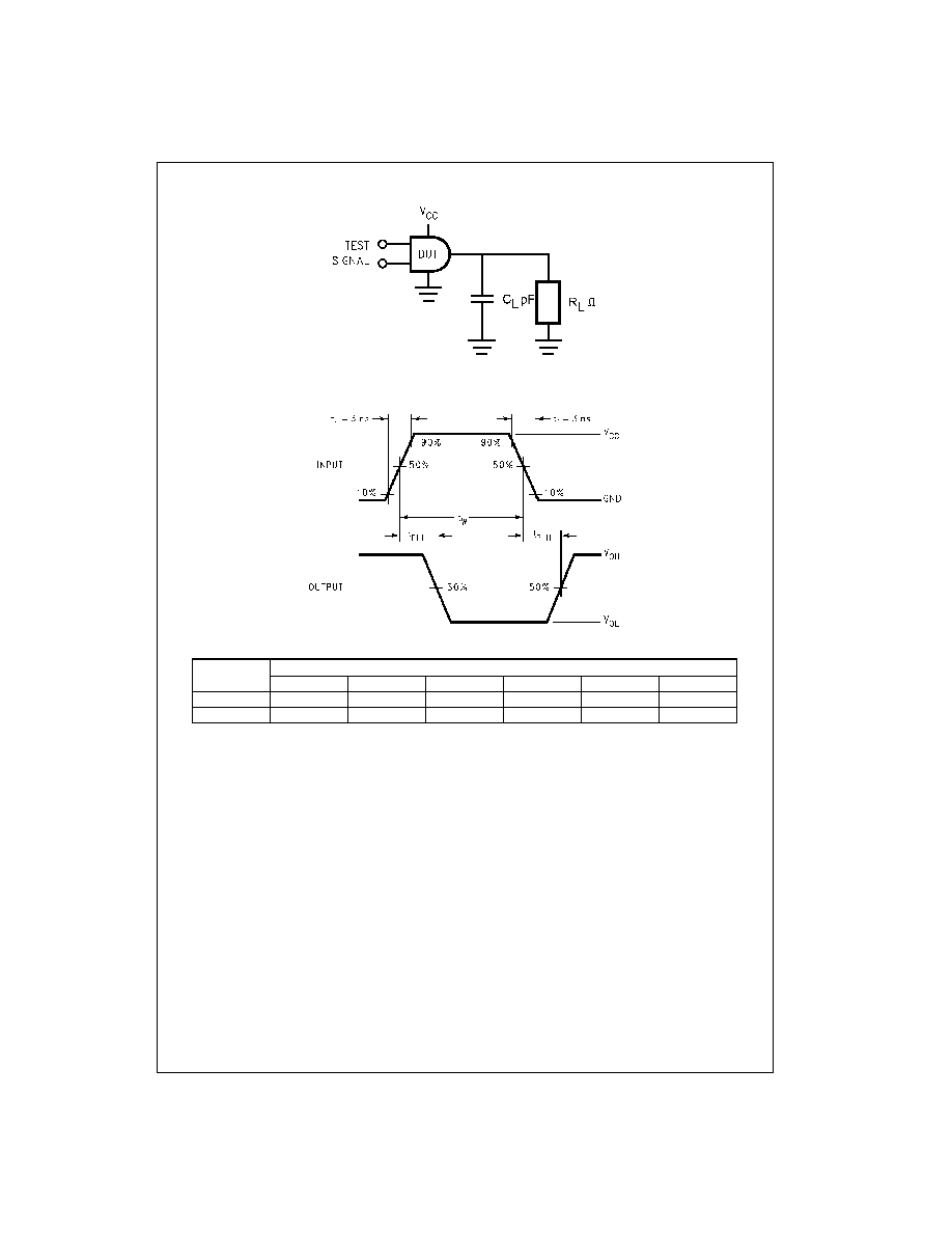
AC Loading and Waveforms
FIGURE 1. AC Test Circuit
FIGURE 2. AC Waveforms
Symbol
V
CC
3.3V
±
0.3V
2.5V
±
0.2V
1.8V
±
0.15V
1.5V
±
0.10V
1.2V
±
0.10V
0.9V
V
mi
1.5V
V
CC
/2
V
CC
/2
V
CC
/2
V
CC
/2
V
CC
/2
V
mo
1.5V
V
CC
/2
V
CC
/2
V
CC
/2
V
CC
/2
V
CC
/2
www.fairchildsemi.com
6
NC7W
P
86
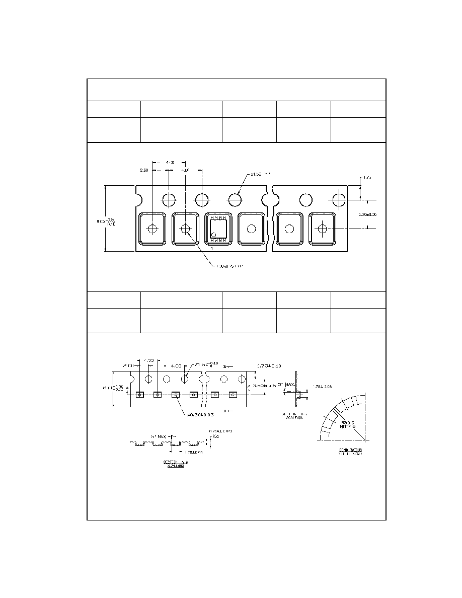
Tape and Reel Specification
TAPE FORMAT for US8
TAPE DIMENSIONS inches (millimeters)
TAPE FORMAT for MicroPak
TAPE DIMENSIONS inches (millimeters)
Package
Tape
Number
Cavity
Cover Tape
Designator
Section
Cavities
Status
Status
Leader (Start End)
125 (typ)
Empty
Sealed
K8X
Carrier
3000
Filled
Sealed
Trailer (Hub End)
75 (typ)
Empty
Sealed
Package
Tape
Number
Cavity
Cover Tape
Designator
Section
Cavities
Status
Status
Leader (Start End)
125 (typ)
Empty
Sealed
L8X
Carrier
3000
Filled
Sealed
Trailer (Hub End)
75 (typ)
Empty
Sealed
7
www.fairchildsemi.com
NC7WP86
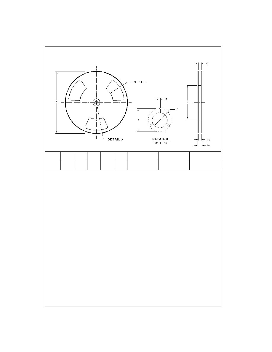
Tape and Reel Specification
(Continued)
REEL DIMENSIONS inches (millimeters)
Tape
Size
A
B
C
D
N
W1
W2
W3
8 mm
7.0
0.059
0.512
0.795
2.165
0.331
+
0.059/
-
0.000
0.567
W1
+
0.078/
-
0.039
(177.8)
(1.50)
(13.00)
(20.20)
(55.00)
(8.40
+
1.50/
-
0.00)
(14.40)
(W1
+
2.00/
-
1.00)
www.fairchildsemi.com
8
NC7W
P
86
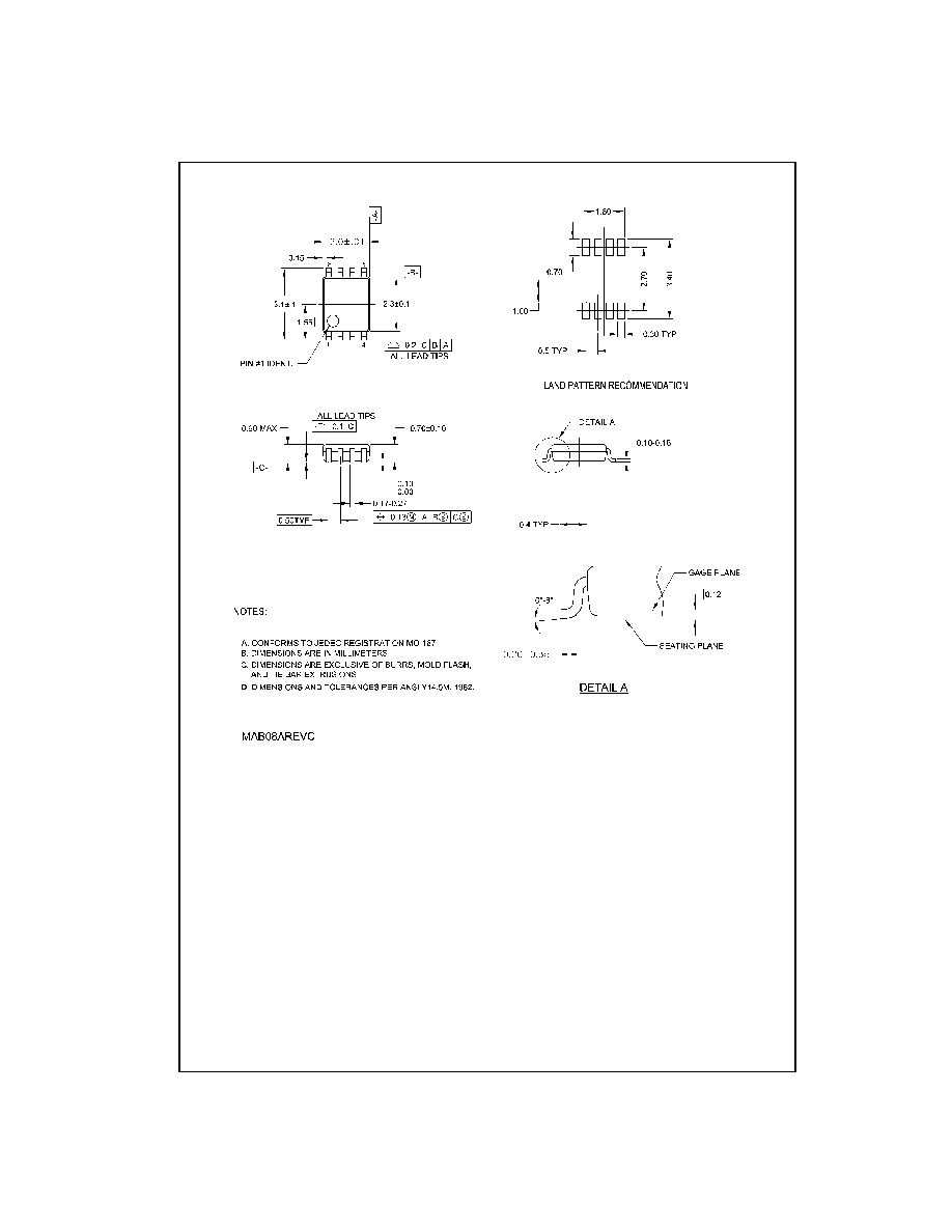
Physical Dimensions
inches (millimeters) unless otherwise noted
8-Lead US8, JEDEC MO-187, Variation CA 3.1mm Wide
Package Number MAB08A
9
www.fairchildsemi.com
NC7WP86 T
i
nyLogi
c
ULP
Dual
2-I
nput Excl
usive
OR
Gat
e
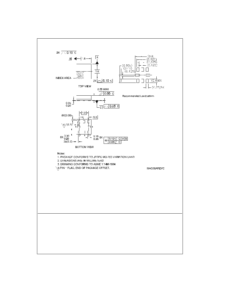
Physical Dimensions
inches (millimeters) unless otherwise noted (Continued)
Pb-Free 8-Lead MicroPak, 1.6 mm Wide
Package Number MAC08A
Fairchild does not assume any responsibility for use of any circuitry described, no circuit patent licenses are implied and
Fairchild reserves the right at any time without notice to change said circuitry and specifications.
LIFE SUPPORT POLICY
FAIRCHILD'S PRODUCTS ARE NOT AUTHORIZED FOR USE AS CRITICAL COMPONENTS IN LIFE SUPPORT
DEVICES OR SYSTEMS WITHOUT THE EXPRESS WRITTEN APPROVAL OF THE PRESIDENT OF FAIRCHILD
SEMICONDUCTOR CORPORATION. As used herein:
1. Life support devices or systems are devices or systems
which, (a) are intended for surgical implant into the
body, or (b) support or sustain life, and (c) whose failure
to perform when properly used in accordance with
instructions for use provided in the labeling, can be rea-
sonably expected to result in a significant injury to the
user.
2. A critical component in any component of a life support
device or system whose failure to perform can be rea-
sonably expected to cause the failure of the life support
device or system, or to affect its safety or effectiveness.
www.fairchildsemi.com