© 2003 Fairchild Semiconductor Corporation
DS500270
www.fairchildsemi.com
April 2000
Revised June 2003
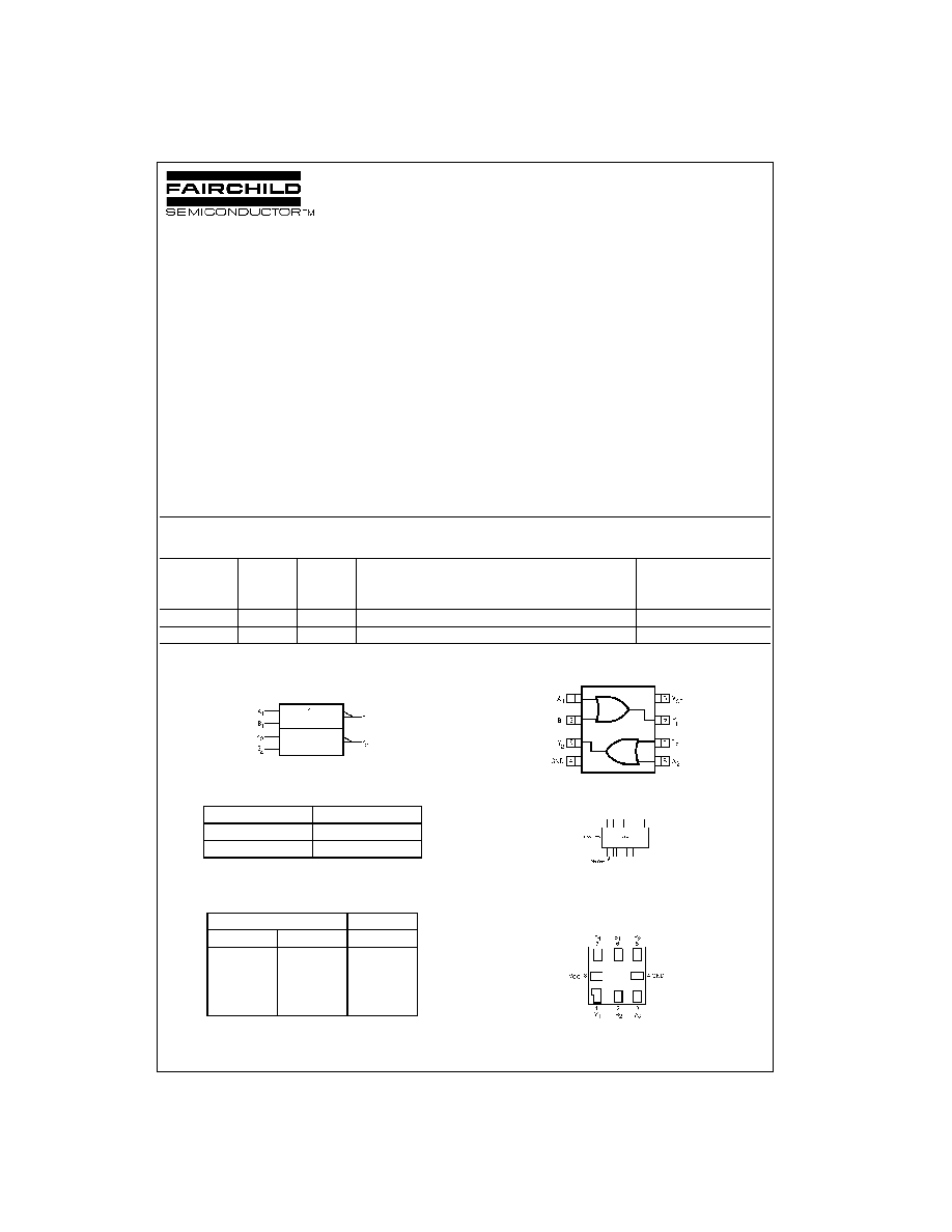
NC7WZ32 T
i
nyLogi
c
UHS Dual
2-I
nput
OR Gat
e
NC7WZ32
TinyLogic
UHS Dual 2-Input OR Gate
General Description
The NC7WZ32 is a dual 2-Input OR Gate from Fairchild's
Ultra High Speed Series of TinyLogic
. The device is fabri-
cated with advanced CMOS technology to achieve ultra
high speed with high output drive while maintaining low
static power dissipation over a very broad V
CC
operating
range. The device is specified to operate over the 1.65V to
5.5V V
CC
range. The inputs and output are high impedance
when V
CC
is 0V. Inputs tolerate voltages up to 7V indepen-
dent of V
CC
operating voltage.
Features
s
Space saving US8 surface mount package
s
MicroPak
leadless package
s
Ultra high speed t
PD
2.4 ns Typ into 50 pF at 5V V
CC
s
High output drive
±
24 mA at 3V V
CC
s
Broad V
CC
operating range 1.65V to 5.5V
s
Matches the performance of LCX when operated at
3.3V V
CC
s
Power down high impedance inputs/output
s
Overvoltage tolerant inputs facilitate 5V to 3V translation
s
Patented noise/EMI reduction circuitry implemented
Ordering Code:
Logic Symbol
IEEE/IEC
Pin Descriptions
Function Table
H
=
HIGH Logic Level
L
=
LOW Logic Level
Connection Diagrams
(Top View)
Pin One Orientation Diagram
AAA represents Product Code Top Mark - see ordering code
Note: Orientation of Top Mark determines Pin One location. Read the top
product code mark left to right, Pin One is the lower left pin (see diagram).
Pad Assignments for MicroPak
(Top Thru View)
TinyLogic
is a registered trademark of Fairchild Semiconductor Corporation.
MIcroPak
is a trademark of Fairchild Semiconductor Corporation.
Product
Package Description
Supplied As
Order
Package
Code
Number
Number
Top Mark
NC7WZ32K8X
MAB08A
WZ32
8-Lead US8, JEDEC MO-187, Variation CA 3.1mm Wide 3k Units on Tape and Reel
NC7WZ32L8X
MAC08A
N5
8-Lead MicroPak, 1.6 mm Wide
5k Units on Tape and Reel
Pin Names
Description
A
n
, B
n
Inputs
Y
n
Output
Y
=
A
+
B
Input
Output
A
B
Y
L
L
L
L
H
H
H
L
H
H
H
H
www.fairchildsemi.com
2
NC7W
Z32
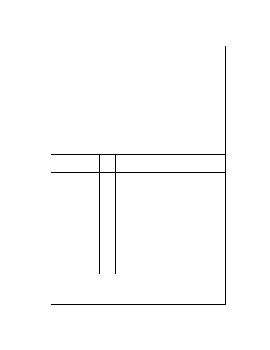
Absolute Maximum Ratings
(Note 1)
Recommended Operating
Conditions
(Note 2)
Note 1: Absolute Maximum Ratings are DC values beyond which the
device may be damaged or have its useful life impaired. The datasheet
specifications should be met, without exception, to ensure that the system
design is reliable over its power supply, temperature, and output/input load-
ing variables. Fairchild does not recommend operation outside datasheet
specifications.
Note 2: Unused inputs must be held HIGH or LOW. They may not float.
DC Electrical Characteristics
Supply Voltage (V
CC
)
-
0.5Vto
+
7V
DC Input Voltage (V
IN
)
-
0.5V to
+
7V
DC Output Voltage (V
OUT
)
-
0.5V to
+
7V
DC Input Diode Current (I
IK
)
@V
IN
<
-
0.5V
-
50 mA
DC Output Diode Current (I
OK
)
@V
OUT
<
-
0.5V
-
50 mA
DC Output Current (I
OUT
)
±
50 mA
DC V
CC
/GND Current (I
CC
/I
GND
)
±
100 mA
Storage Temperature (T
STG
)
-
65
∞
C to
+
150
∞
C
Junction Temperature under Bias (T
J
)
150
∞
C
Junction Lead Temperature (T
L
);
Soldering, 10 seconds
260
∞
C
Power Dissipation (P
D
) @
+
85
∞
C
250 mW
Supply Voltage Operating (V
CC
)
1.65V to 5.5
Supply Voltage Data Retention (V
CC
)
1.5V to 5.5V
Input Voltage (V
IN
)
0V to 5.5V
Output Voltage (V
OUT
)
0V to V
CC
Operating Temperature (T
A
)
-
40
∞
C to
+
85
∞
C
Input Rise and Fall Time (t
r
, t
f
)
V
CC
=
1.80V
±
0.15V, 2.5V
±
0.2V
0 ns/V to 20 ns/V
V
CC
=
3.3V
±
0.3V
0 ns/V to 10 ns/V
V
CC
=
5.0V
±
0.5V
0 ns/V to 5 ns/V
Thermal Resistance (
JA
)
250
∞
C/W
Symbol
Parameter
V
CC
T
A
=
+
25
∞
C
T
A
=
-
40
∞
C to
+
85
∞
C
Units
Conditions
(V)
Min
Typ
Max
Min
Max
V
IH
HIGH Level Input Voltage
1.65 to 1.95 0.75 V
CC
0.75 V
CC
V
2.3 to 5.5
0.7 V
CC
0.7 V
CC
V
IL
LOW Level Input Voltage
1.65 to 1.95
0.25 V
CC
0.25 V
CC
V
2.3 to 5.5
0.3 V
CC
0.3 V
CC
V
OH
HIGH Level Output Voltage
1.65
1.55
1.65
1.55
V
V
IN
=
V
IH
I
OH
=
≠100
µ
A
2.3
2.2
2.3
2.2
3.0
2.9
3.0
2.9
4.5
4.4
4.5
4.4
1.65
1.29
1.52
1.29
V
I
OH
=
-
4 mA
2.3
1.9
2.15
1.9
I
OH
=
-
8 mA
3.0
2.4
2.80
2.4
I
OH
=
-
16 mA
3.0
2.3
2.68
2.3
I
OH
=
-
24 mA
4.5
3.8
4.20
3.8
I
OH
=
-
32 mA
V
OL
LOW Level Output Voltage
1.65
0.0
0.1
0.1
V
V
IN
=
V
IL
I
OL
=
100
µ
A
2.3
0.0
0.1
0.1
3.0
0.0
0.1
0.1
4.5
0.0
0.1
0.1
1.65
0.08
0.24
0.24
V
I
OL
=
4 mA
2.3
0.10
0.3
0.3
I
OL
=
8 mA
3.0
0.15
0.4
0.4
I
OL
=
16 mA
3.0
0.22
0.55
0.55
I
OL
=
24 mA
4.5
0.22
0.55
0.55
I
OL
=
32 mA
I
IN
Input Leakage Current
0 to 5.5
±
0.1
±
1
µ
A
V
IN
=
5.5V, GND
I
OFF
Power Off Leakage Current
0.0
1
10
µ
A
V
IN
or V
OUT
=
5.5V
I
CC
Quiescent Supply Current
1.65 to 5.5
1
10
µ
A
V
IN
=
5.5V, GND
3
www.fairchildsemi.com
NC7WZ32
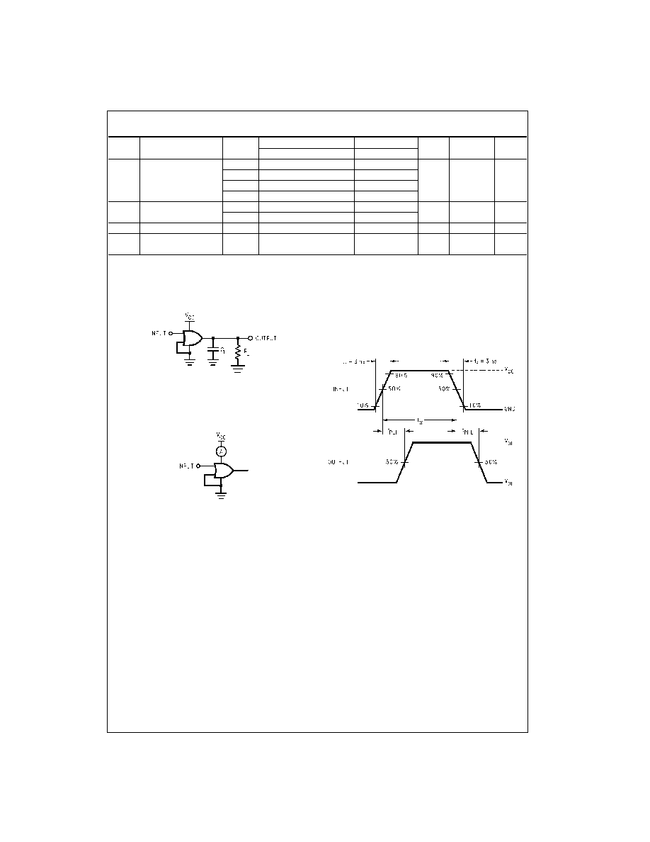
AC Electrical Characteristics
Note 3: C
PD
is defined as the value of the internal equivalent capacitance which is derived from dynamic operating current consumption (I
CCD
) at no output
loading and operating at 50% duty cycle. (See Figure 2.) C
PD
is related to I
CCD
dynamic operating current by the expression:
I
CCD
=
(C
PD
) (V
CC
) (f
IN
)
+
(I
CC
static).
AC Loading and Waveforms
C
L
includes load and stray capacitance.
Input PRR
=
1.0 MHz, t
w
=
500 ns.
FIGURE 1. AC Test Circuit
Input
=
AC Waveforms; t
r
=
t
f
=
1.8 ns;
PRR
=
10 MHz; Duty Cycle
=
50%
FIGURE 2. I
CCD
Test Circuit
FIGURE 3. AC Waveforms
Symbol
Parameter
V
CC
T
A
=
+
25
∞
C
T
A
=
-
40
∞
C to
+
85
∞
C
Units
Conditions
Figure
(V)
Min
Typ
Max
Min
Max
Number
t
PLH
,
Propagation Delay
1.8
±
0.15
2.0
5.8
10.5
2.0
11.0
ns
t
PHL
2.5
±
0.2
1.0
3.5
5.8
1.0
6.2
C
L
= 15 pF,
Figures
1, 3
3.3
±
0.3
0.8
2.6
3.9
0.8
4.3
R
L
= 1M
5.0
±
0.5
0.5
1.8
3.1
0.5
3.3
t
PLH
,
Propagation Delay
3.3
±
0.3
1.2
3.2
4.8
1.2
5.2
ns
C
L
= 50 pF,
Figures
1, 3
t
PHL
5.0
±
0.5
0.8
2.4
3.7
0.8
4.0
R
L
= 500
C
IN
Input Capacitance
0
2.5
pF
C
PD
Power Dissipation
3.3
14
pF
(Note 3)
Figure 2
Capacitance
5.0
18