 | ÐлекÑÑоннÑй компоненÑ: NDB6060 | СкаÑаÑÑ:  PDF PDF  ZIP ZIP |
Äîêóìåíòàöèÿ è îïèñàíèÿ www.docs.chipfind.ru
March 1996
NDP6060 / NDB6060
N-Channel Enhancement Mode Field Effect Transistor
General Description
Features
________________________________________________________________________________
Absolute Maximum Ratings
T
C
= 25°C unless otherwise noted
Symbol
Parameter
NDP6060
NDB6060
Units
V
DSS
Drain-Source Voltage
60
V
V
DGR
Drain-Gate Voltage (R
GS
< 1 M
)
60
V
V
GSS
Gate-Source Voltage - Continuous
± 20
V
- Nonrepetitive (t
P
< 50 µs)
± 40
I
D
Drain Current
- Continuous T
c
=25
o
C
48
A
- Continuous T
C
=100
o
C
32
- Pulsed
144
P
D
Total Power Dissipation @ T
C
= 25°C
100
W
Derate above 25°C
0.67
W/°C
T
J
,T
STG
Operating and Storage Temperature Range
-65 to 175
°C
T
L
Maximum lead temperature for soldering purposes,
1/8" from case for 5 seconds
275
°C
NDP6060 Rev. B1 / NDB6060 Rev. C
These N-Channel enhancement mode power field effect
transistors are produced using Fairchild's proprietary, high
cell density, DMOS technology. This very high density
process has been especially tailored to minimize on-state
resistance, provide superior switching performance, and
withstand high energy pulses in the avalanche and
commutation modes. These devices are particularly suited
for low voltage applications such as automotive, DC/DC
converters, PWM motor controls, and other battery
powered circuits where fast switching, low in-line power
loss, and resistance to transients are needed.
48A, 60V. R
DS(ON)
= 0.025
@ V
GS
=10V.
Critical DC electrical parameters specified at elevated
temperature.
Rugged internal source-drain diode can eliminate the need
for an external Zener diode transient suppressor.
175°C maximum junction temperature rating.
High density cell design for extremely low R
DS(ON)
.
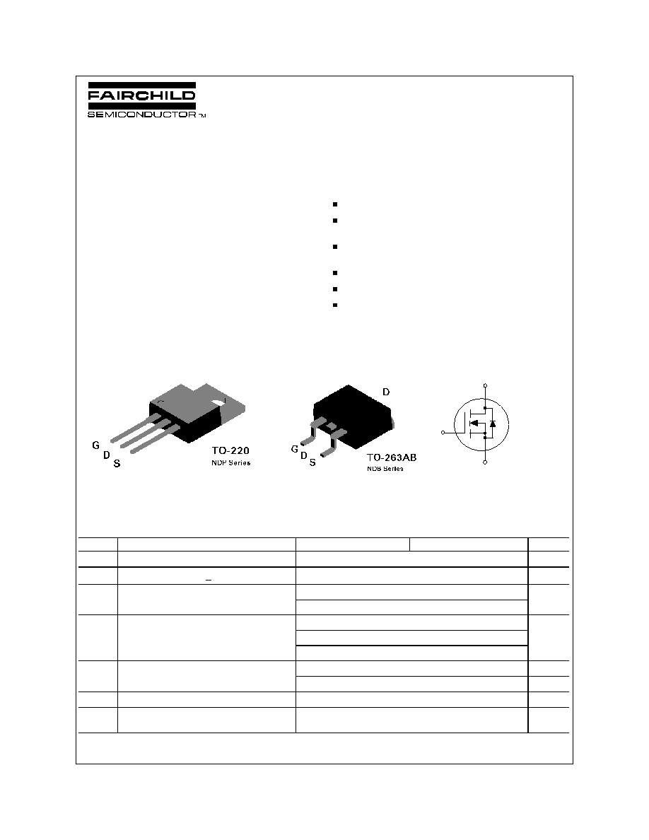
TO-220 and TO-263 (D
2
PAK) package for both through hole
and surface mount applications.
S
D
G
© 1997 Fairchild Semiconductor Corporation
Electrical Characteristics
(T
C
= 25°C unless otherwise noted)
Symbol
Parameter
Conditions
Min
Typ
Max
Units
DRAIN-SOURCE AVALANCHE RATINGS
(Note 1)
W
DSS
Single Pulse Drain-Source Avalanche
Energy
V
DD
= 25 V, I
D
= 48 A
200
mJ
I
AR
Maximum Drain-Source Avalanche Current
48
A
OFF CHARACTERISTICS
BV
DSS
Drain-Source Breakdown Voltage
V
GS
= 0 V, I
D
= 250 µA
60
V
I
DSS
Zero Gate Voltage Drain Current
V
DS
= 60 V, V
GS
= 0 V
250
µA
T
J
= 125°C
1
mA
I
GSSF
Gate - Body Leakage, Forward
V
GS
= 20 V, V
DS
= 0 V
100
nA
I
GSSR
Gate - Body Leakage, Reverse
V
GS
= -20 V, V
DS
= 0 V
-100
nA
ON CHARACTERISTICS
(Note 1)
V
GS(th)
Gate Threshold Voltage
V
DS
= V
GS
, I
D
= 250 µA
2
2.9
4
V
T
J
= 125°C
1.4
2.3
3.6
R
DS(ON)
Static Drain-Source On-Resistance
V
GS
= 10 V, I
D
= 24 A
0.02
0.025
T
J
= 125°C
0.032
0.04
I
D(on)
On-State Drain Current
V
GS
= 10 V, V
DS
= 10 V
48
A
g
FS
Forward Transconductance
V
DS
= 10 V, I
D
= 24 A
10
19
S
DYNAMIC CHARACTERISTICS
C
iss
Input Capacitance
V
DS
= 25 V, V
GS
= 0 V,
f = 1.0 MHz
1190
1800
pF
C
oss
Output Capacitance
475
800
pF
C
rss
Reverse Transfer Capacitance
150
400
pF
SWITCHING CHARACTERISTICS
(Note 1)
t
D(on)
Turn - On Delay Time
V
DD
= 30 V, I
D
= 48 A,
V
GS
= 10 V, R
GEN
= 7.5
10
20
nS
t
r
Turn - On Rise Time
145
300
nS
t
D(off)
Turn - Off Delay Time
28
60
nS
t
f
Turn - Off Fall Time
77
150
nS
Q
g
Total Gate Charge
V
DS
= 48 V,
I
D
= 48 A, V
GS
= 10V
39
70
nC
Q
gs
Gate-Source Charge
7.6
nC
Q
gd
Gate-Drain Charge
22
nC
NDP6060 Rev. B1 / NDB6060 Rev. C
Electrical Characteristics
(T
C
= 25°C unless otherwise noted)
Symbol
Parameter
Conditions
Min
Typ
Max
Units
DRAIN-SOURCE DIODE CHARACTERISTICS
I
S
Maximum Continuos Drain-Source Diode Forward Current
48
A
I
SM
Maximum Pulsed Drain-Source Diode Forward Current
144
A
V
SD
Drain-Source Diode Forward Voltage
V
GS
= 0 V, I
S
= 24 A
(Note 1)
0.9
1.3
V
T
J
= 125°C
0.8
1.2
t
rr
Reverse Recovery Time
V
GS
= 0 V, I
F
= 48 A,
dI
F
/dt = 100 A/µs
35
87
140
ns
I
rr
Reverse Recovery Current
2
3.6
8
A
THERMAL CHARACTERISTICS
R
JC
Thermal Resistance, Junction-to-Case
1.5
°C/W
R
JA
Thermal Resistance, Junction-to-Ambient
62.5
°C/W
Note:
1. Pulse Test: Pulse Width < 300 µs, Duty Cycle < 2.0%.
NDP6060 Rev. B1 / NDB6060 Rev. C
NDP6060 Rev. B1 / NDB6060 Rev. C
0
1
2
3
4
5
6
0
20
40
60
80
100
V , DRAIN-SOURCE VOLTAGE (V)
I , DRAIN-SOURCE CURRENT (A)
V = 20V
GS
DS
D
6.0
5.0
7.0
8.0
10
12
9.0
-50
-25
0
25
50
75
1 0 0
1 2 5
1 5 0
1 7 5
0.5
0.75
1
1.25
1.5
1.75
2
T , JUNCTION TEMPERATURE (°C)
DRAIN-SOURCE ON-RESISTANCE
J
V = 10V
GS
I = 24A
D
R , NORMALIZED
DS(ON)
-50
-25
0
25
50
75
100
125
150
175
0.5
0.6
0.7
0.8
0.9
1
1.1
1.2
T , JUNCTION TEMPERATURE (°C)
GATE-SOURCE THRESHOLD VOLTAGE
J
V , NORMALIZED
GS(th)
I = 250µA
D
V = V
GS
DS
0
20
40
60
80
100
0.6
0.8
1
1.2
1.4
1.6
1.8
2
I , DRAIN CURRENT (A)
DRAIN-SOURCE ON-RESISTANCE
D
R , NORMALIZED
DS(on)
V = 6.0V
GS
9.0
10
7.0
8.0
20
12
0
20
40
60
80
100
0.5
1
1.5
2
2.5
I , DRAIN CURRENT (A)
DRAIN-SOURCE ON-RESISTANCE
V = 10V
GS
T = 125°C
J
25°C
-55°C
D
R , NORMALIZED
DS(on)
2
4
6
8
10
0
10
20
30
40
50
60
V , GATE TO SOURCE VOLTAGE (V)
I , DRAIN CURRENT (A)
25°C
125°C
V = 10V
DS
GS
D
T = -55°C
J
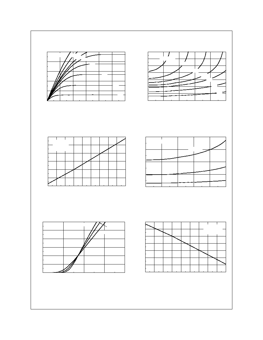
Typical Electrical Characteristics
Figure 1. On-Region Characteristics
Figure 2. On-Resistance Variation with Gate
Voltage and Drain Current
Figure 3. On-Resistance Variation
with Temperature
Figure 4. On-Resistance Variation with Drain
Current and Temperature
Figure 5. Transfer Characteristics
Figure 6. Gate Threshold Variation with
Temperature
NDP6060 Rev. B1 / NDB6060 Rev. C
-50
-25
0
25
50
75
100
125
150
175
0.9
0.95
1
1.05
1.1
1.15
T , JUNCTION TEMPERATURE (°C)
DRAIN-SOURCE BREAKDOWN VOLTAGE
I = 250µA
D
BV , NORMALIZED
DSS
J
0.2
0.4
0.6
0.8
1
1.2
1.4
0.0001
0.001
0.01
0.1
1
10
60
V , BODY DIODE FORWARD VOLTAGE (V)
I , REVERSE DRAIN CURRENT (A)
V = 0V
GS
T = 125°C
J
25°C
-55°C
SD
S
0
20
4 0
6 0
80
0
5
1 0
1 5
2 0
Q , GATE CHARGE (nC)
V , GATE-SOURCE VOLTAGE (V)
g
GS
48V
I = 48A
D
V = 12V
DS
24V
1
2
3
5
1 0
20
30
50
1 0 0
2 0 0
3 0 0
5 0 0
1 0 0 0
2 0 0 0
3 0 0 0
V , DRAIN TO SOURCE VOLTAGE (V)
CAPACITANCE (pF)
DS
f = 1 MHz
V = 0V
GS
C
oss
C
iss
C
rss
G
D
S
V
DD
R
L
V
V
IN
OUT
V
GS
DUT
R
GEN
1 0 %
5 0 %
9 0 %
1 0 %
9 0 %
9 0 %
5 0 %
V
IN
V
O U T
o n
off
d(off)
f
r
d(on)
t
t
t
t
t
t
INVERTED
1 0 %
PULSE W IDTH
Figure 7. Breakdown Voltage Variation with
Temperature
Figure 8. Body Diode Forward Voltage Variation
with Current and Temperature
Figure 9. Capacitance Characteristics
Figure 10. Gate Charge Characteristics
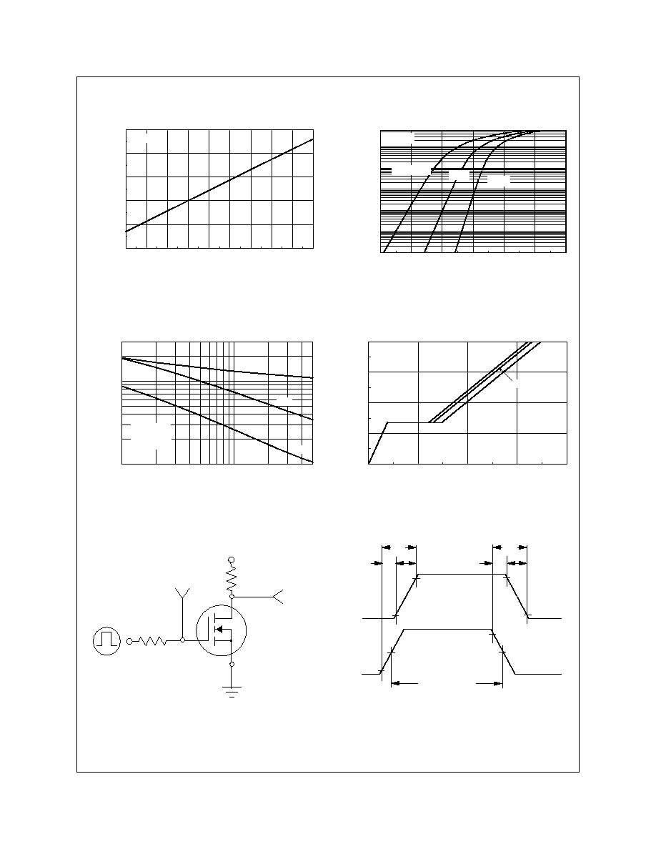
Figure 11. Switching Test Circuit
Figure 12. Switching Waveforms
Typical Electrical Characteristics
(continued)