 | ÐлекÑÑоннÑй компоненÑ: NDH831N | СкаÑаÑÑ:  PDF PDF  ZIP ZIP |
Äîêóìåíòàöèÿ è îïèñàíèÿ www.docs.chipfind.ru
July 1996
NDH831N
N-Channel Enhancement Mode Field Effect Transistor
General Description
Features
____________________________________________________________________________________________
Absolute Maximum Ratings T
A
= 25°C unless otherwise noted
Symbol
Parameter
NDH831N
Units
V
DSS
Drain-Source Voltage
20
V
V
GSS
Gate-Source Voltage
8
V
I
D
Drain Current - Continuous
(Note 1a)
5.8
A
- Pulsed
20
P
D
Maximum Power Dissipation
(Note 1a)
1.8
W
(Note 1b)
1
(Note 1c)
0.9
T
J
,T
STG
Operating and Storage Temperature Range
-55 to 150
°C
THERMAL CHARACTERISTICS
R
JA
Thermal Resistance, Junction-to-Ambient
(Note 1a)
70
°C/W
R
JC
Thermal Resistance, Junction-to-Case
(Note 1)
20
°C/W
NDH831N Rev. D
These N-Channel enhancement mode power field effect
transistors are produced using Fairchild's proprietary, high cell
density, DMOS technology. This very high density process is
especially tailored to minimize on-state resistance and provide
superior switching performance. These devices are particularly
suited for low voltage applications such as notebook computer
power management and portable electronics where fast
switching, low in-line power loss, and resistance to transients
are needed.
5.8A, 20V. R
DS(ON)
= 0.03
@ V
GS
= 4.5V
R
DS(ON)
= 0.04
@ V
GS
= 2.7V.
High density cell design for extremely low R
DS(ON)
.
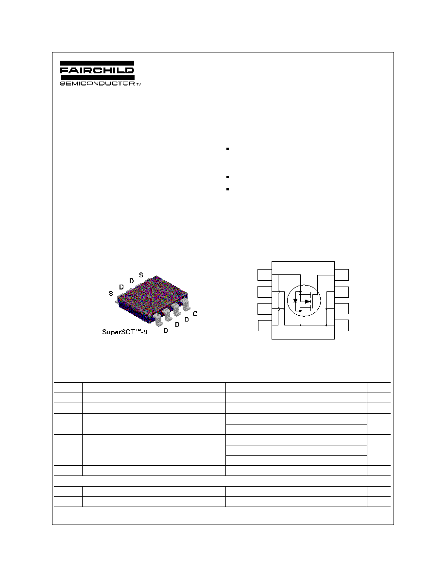
Enhanced SuperSOT
TM
-8 small outline surface mount
package with high power and current handling capability.
1
5
6
7
8
4
3
2
© 1997 Fairchild Semiconductor Corporation
ELECTRICAL CHARACTERISTICS (T
A
= 25°C unless otherwise noted)
Symbol
Parameter
Conditions
Min
Typ
Max
Units
OFF CHARACTERISTICS
BV
DSS
Drain-Source Breakdown Voltage
V
GS
= 0 V, I
D
= 250 µA
20
V
I
DSS
Zero Gate Voltage Drain Current
V
DS
= 16 V, V
GS
= 0 V
1
µA
T
J
= 55°C
10
µA
I
GSSF
Gate - Body Leakage, Forward
V
GS
= 8 V, V
DS
= 0 V
100
nA
I
GSSR
Gate - Body Leakage, Reverse
V
GS
= -8 V, V
DS
= 0 V
-100
nA
ON CHARACTERISTICS
(Note 2)
V
GS(th)
Gate Threshold Voltage
V
DS
= V
GS
, I
D
= 250 µA
0.4
0.6
1
V
T
J
= 125°C
0.3
0.35
0.8
R
DS(ON)
Static Drain-Source On-Resistance
V
GS
= 4.5 V, I
D
= 5.8 A
0.022
0.03
W
T
J
= 125°C
0.03
0.54
V
GS
= 2.7 V, I
D
= 5 A
0.027
0.04
I
D(on)
On-State Drain Current
V
GS
= 4.5 V, V
DS
= 5 V
20
A
V
GS
= 2.7 V, V
DS
= 5 V
5
g
FS
Forward Transconductance
V
DS
= 10 V, I
D
= 5.8 A
14
S
DYNAMIC CHARACTERISTICS
C
iss
Input Capacitance
V
DS
= 10 V, V
GS
= 0 V,
f = 1.0 MHz
720
pF
C
oss
Output Capacitance
430
pF
C
rss
Reverse Transfer Capacitance
155
pF
SWITCHING CHARACTERISTICS
(Note 2)
t
D(on)
Turn - On Delay Time
V
DD
= 6 V, I
D
= 1 A,
V
GEN
= 4.5 V, R
GEN
= 6
10
20
ns
t
r
Turn - On Rise Time
30
50
ns
t
D(off)
Turn - Off Delay Time
55
80
ns
t
f
Turn - Off Fall Time
20
40
ns
Q
g
Total Gate Charge
V
DS
= 5 V,
I
D
= 5.8 A, V
GS
= 4.5 V
19.5
28
nC
Q
gs
Gate-Source Charge
1.8
nC
Q
gd
Gate-Drain Charge
5.5
nC
NDH831N Rev. D
ELECTRICAL CHARACTERISTICS (T
A
= 25°C unless otherwise noted)
Symbol
Parameter
Conditions
Min
Typ
Max
Units
DRAIN-SOURCE DIODE CHARACTERISTICS AND MAXIMUM RATINGS
I
S
Maximum Continuous Drain-Source Diode Forward Current
1.5
A
V
SD
Drain-Source Diode Forward Voltage
V
GS
= 0 V, I
S
= 1.5 A
(Note 2)
0.75
1.2
V
Notes:
1. R
JA
is the sum of the junction-to-case and case-to-ambient thermal resistance where the case thermal reference is defined as the solder mounting surface of the drain pins. R
JC
is guaranteed by
design while R
CA
is determined by the user's board design.
P
D
(
t
) =
T
J
-
T
A
R
J A
(
t
)
=
T
J
-
T
A
R
J C
+
R
CA
(
t
)
=
I
D
2
(
t
) ×
R
DS
(
ON
)
T
J
Typical R
qJA
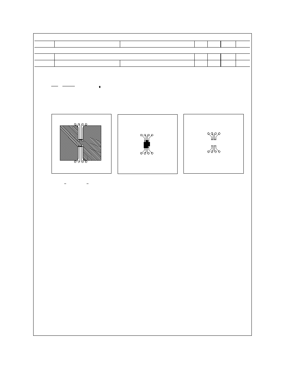
using the board layouts shown below on 4.5"x5" FR-4 PCB in a still air environment:
a. 70
o
C/W when mounted on a 1 in
2
pad of 2oz copper.
b. 125
o
C/W when mounted on a 0.026 in
2
pad of 2oz copper.
c. 135
o
C/W when mounted on a 0.005 in
2
pad of 2oz copper.
Scale 1 : 1 on letter size paper
2. Pulse Test: Pulse Width < 300µs, Duty Cycle < 2.0%.
NDH831N Rev. D
1a
1b
1c
NDH831N Rev. D
0
0.5
1
1.5
2
2.5
3
0
5
10
15
20
25
30
V , DRAIN-SOURCE VOLTAGE (V)
I , DRAIN-SOURCE CURRENT (A)
3.5
3.0
2.7
V =4.5V
GS
DS
D
2.5
1.5
2.0
-50
-25
0
25
50
75
100
125
150
0.6
0.8
1
1.2
1.4
1.6
T , JUNCTION TEMPERATURE (°C)
DRAIN-SOURCE ON-RESISTANCE
J
V = 4.5V
GS
I = 5.8A
D
R , NORMALIZED
DS(ON)
0
5
10
15
20
25
30
0.8
1
1.2
1.4
1.6
1.8
2
I , DRAIN CURRENT (A)
DRAIN-SOURCE ON-RESISTANCE
V = 2.0V
GS
D
R , NORMALIZED
DS(on)
3.5
4 .0
2 .7
3 .0
2 .5
5.0
4 .5
0
5
10
15
20
25
30
0.5
1
1.5
2
I , DRAIN CURRENT (A)
DRAIN-SOURCE ON-RESISTANCE
T = 125°C
J
25°C
D
V = 4.5 V
GS
-55°C
R , NORMALIZED
DS(on)
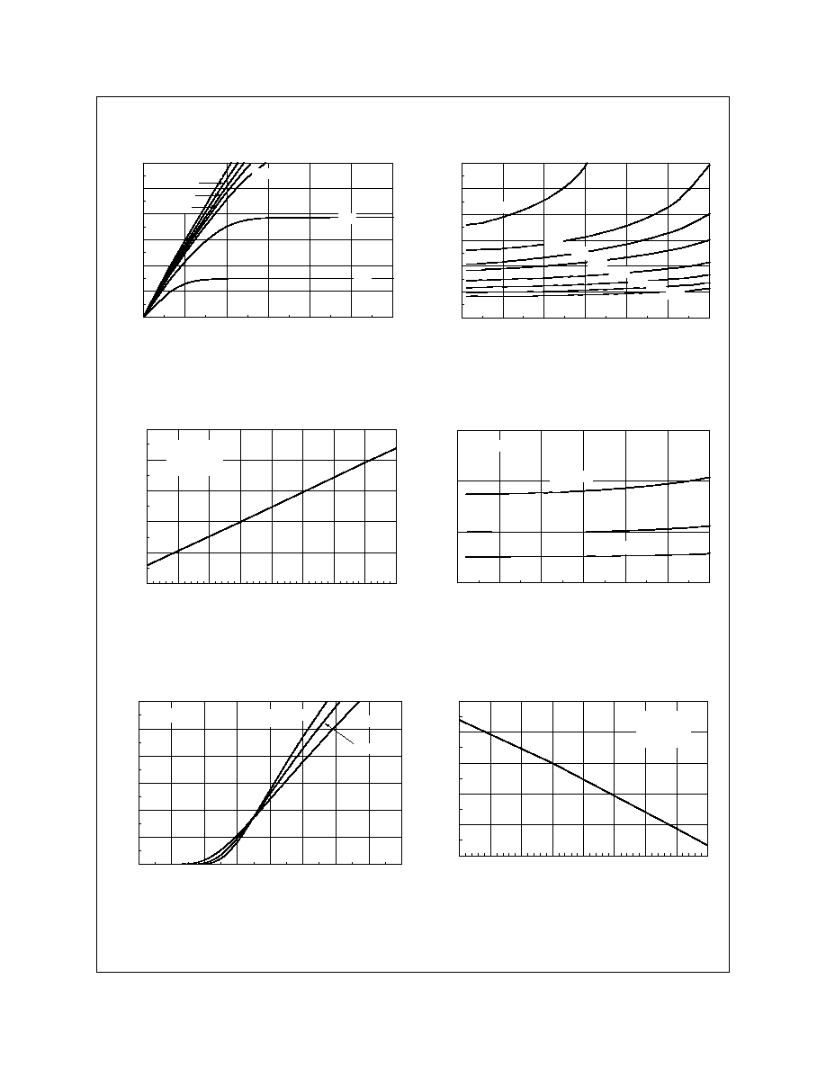
Typical Electrical Characteristics
Figure 1. On-Region Characteristics.
Figure 2. On-Resistance Variation with Gate
Voltage and Drain Current.
Figure 3. On-Resistance Variation with
Temperature.
Figure 4. On-Resistance Variation with Drain
Current and Temperature.
Figure 5. Transfer Characteristics.
Figure 6. Gate Threshold Variation with
Temperature.
0
0.5
1
1.5
2
2.5
3
3.5
4
0
5
10
15
20
25
30
V , GATE TO SOURCE VOLTAGE (V)
I , DRAIN CURRENT (A)
25°C
125°C
V = 5.0V
DS
GS
D
T = -55°C
J
-50
-25
0
25
50
75
1 0 0
1 2 5
1 5 0
0.4
0.6
0.8
1
1.2
1.4
T , JUNCTION TEMPERATURE (°C)
GATE-SOURCE THRESHOLD VOLTAGE
J
I = 250µA
D
V = V
DS
GS
V , NORMALIZED
th
NDH831N Rev. D
-50
-25
0
25
50
75
100
125
150
0.92
0.96
1
1.04
1.08
1.12
T , JUNCTION TEMPERATURE (°C)
DRAIN-SOURCE BREAKDOWN VOLTAGE
I = 250µA
D
BV , NORMALIZED
DSS
J
0
0.2
0.4
0.6
0.8
1
1.2
1.4
0.0001
0.001
0.01
0.1
1
5
1 0
3 0
V , BODY DIODE FORWARD VOLTAGE (V)
I , REVERSE DRAIN CURRENT (A)
T = 125°C
J
25°C
-55°C
V = 0V
GS
SD
S
0
5
10
15
20
25
0
1
2
3
4
5
Q , GATE CHARGE (nC)
V , GATE-SOURCE VOLTAGE (V)
g
GS
I = 5.8A
D
10V
15V
V = 5V
DS
0.1
0.2
0.5
1
2
5
1 0
20
1 0 0
2 0 0
3 0 0
5 0 0
1 0 0 0
2 0 0 0
3 0 0 0
V , DRAIN TO SOURCE VOLTAGE (V)
CAPACITANCE (pF)
DS
C iss
f = 1 MHz
V = 0V
GS
C oss
C rss
Figure 7. Breakdown Voltage Variation with
Temperature.
Figure 8. Body Diode Forward Voltage Variation
with Current and Temperature
.
Figure 9. Capacitance Characteristics.
Figure 10. Gate Charge Characteristics.
Typical Electrical Characteristics
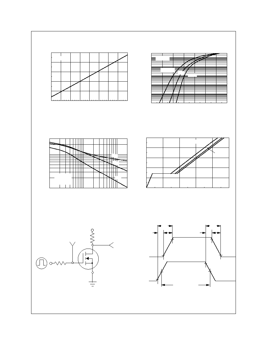
G
D
S
V
DD
R
L
V
V
IN
OUT
V
GS
DUT
R
GEN
Figure 11. Switching Test Circuit
Figure 12. Switching Waveforms
10%
50%
90%
10%
90%
90%
50%
V
IN
V
OUT
on
off
d(off)
f
r
d(on)
t
t
t
t
t
t
INVERTED
10%
PULSE WIDTH