 | –≠–ª–µ–∫—Ç—Ä–æ–Ω–Ω—ã–π –∫–æ–º–ø–æ–Ω–µ–Ω—Ç: NDH8320C | –°–∫–∞—á–∞—Ç—å:  PDF PDF  ZIP ZIP |
December 1996
NDH8320C
Dual N & P-Channel Enhancement Mode Field Effect Transistor
General Description Features
_____________________________________________________________________
______________
Absolute Maximum Ratings
T
A
= 25∞C unless otherwise noted
Symbol Parameter N-Channel P-Channel Units
V
DSS
Drain-Source Voltage 20 -20 V
V
GSS
Gate-Source Voltage 8 -8 V
I
D
Drain Current - Continuous
(Note 1)
3 -2 A
- Pulsed 15 -10
P
D
Power Dissipation for Single Operation
(Note 1)
0.8 W
T
J
,T
STG
Operating and Storage Temperature Range -55 to 150 ∞C
THERMAL CHARACTERISTICS
R
JA
Thermal Resistance, Junction-to-Ambient
(Note 1)
156 ∞C/W
R
JC
Thermal Resistance, Junction-to-Case
(Note 1)
40 ∞C/W
NDH8320C Rev.B
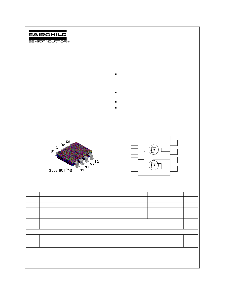
These dual N- and P -Channel enhancement mode power
field effect transistors are produced using Fairchild's
proprietary, high cell density, DMOS technology. This very
high density process is especially tailored to minimize
on-state resistance and provide superior switching
performance. These devices are particularly suited for low
voltage applications such as notebook computer power
management and other battery powered circuits where fast
switching, low in-line power loss, and resistance to
transients are needed.
N-Channel 3 A, 20 V, R
DS(ON)
=0.06
@ V
GS
=4.5 V
R
DS(ON)
=0.075
@ V
GS
=2.7 V P-Channel -2A, -20V,
R
DS(ON)
=0.13
@ V
GS
=-4.5 V
R
DS(ON)
=0.19
@ V
GS
=-2.7 V.
Proprietary SuperSOT
TM
-8 package design using copper lead
frame for superior thermal and electrical capabilities.
High density cell design for extremely low R
DS(ON)
.
Exceptional on-resistance and maximum DC current
capability.
1
5
6
7
8
4
3
2
© 1997 Fairchild Semiconductor Corporation
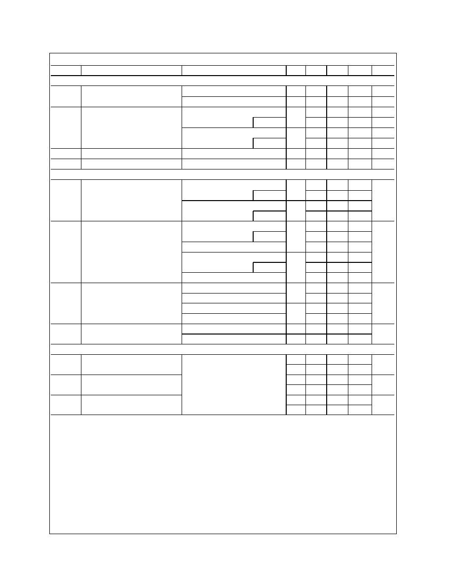
Electrical Characteristics
(T
A
= 25∞C unless otherwise noted)
Symbol
Parameter
Conditions
Type
Min
Typ
Max
Units
OFF CHARACTERISTICS
BV
DSS
Drain-Source Breakdown Voltage
V
GS
= 0 V, I
D
= 250 µA
N-Ch
20
V
V
GS
= 0 V, I
D
= -250 µA
P-Ch
-20
V
I
DSS
Zero Gate Voltage Drain Current
V
DS
= 16 V, V
GS
= 0 V
N-Ch
1
µA
T
J
= 55
o
C
10
µA
V
DS
= -16 V, V
GS
= 0 V
P-Ch
-1
µA
T
J
= 55
o
C
-10
µA
I
GSSF
Gate - Body Leakage, Forward
V
GS
= 8 V, V
DS
= 0 V
All
100
nA
I
GSSR
Gate - Body Leakage, Reverse
V
GS
= -8 V, V
DS
= 0 V
All
-100
nA
ON CHARACTERISTICS
(Note 2)
V
GS(th)
Gate Threshold Voltage
V
DS
= V
GS
, I
D
= 250 µA
N-Ch
0.4
0.7
1
V
T
J
= 125
o
C
0.3
0.45
0.7
V
DS
= V
GS
, I
D
= -250 µA
P-Ch
-0.4
-0.6
-1
T
J
= 125
o
C
-0.3
-0.42
-0.7
R
DS(ON)
Static Drain-Source On-Resistance
V
GS
= 4.5 V, I
D
= 3 A
N-Ch
0.047
0.06
T
J
= 125
o
C
0.07
0.11
V
GS
= 2.7 V, I
D
= 2.6 A
0.059
0.075
V
GS
= -4.5 V, I
D
= -2 A
P-Ch
0.102
0.13
T
J
= 125
o
C
0.15
0.23
V
GS
= -2.7 V, I
D
= -1.7 A
0.147
0.19
I
D(on)
On-State Drain Current
V
GS
= 4.5 V, V
DS
= 5 V
N-Ch
15
A
V
GS
= 2.7 V, V
DS
= 5 V
5
V
GS
= -4.5 V, V
DS
= -5 V
P-Ch
-10
V
GS
= -2.7 V, V
DS
= -5 V
-4
g
FS
Forward Transconductance
V
DS
= 5 V, I
D
= 3 A
N-Ch
10
S
V
DS
= -5 V, I
D
= -2 A
P-Ch
5
DYNAMIC CHARACTERISTICS
C
iss
Input Capacitance
N-Channel
V
DS
= 10 V, V
GS
= 0 V,
f = 1.0 MHz
P-Channel
V
DS
= -10 V, V
GS
= 0 V,
f = 1.0 MHz
N-Ch
415
pF
P-Ch
515
C
oss
Output Capacitance
N-Ch
220
pF
P-Ch
250
C
rss
Reverse Transfer Capacitance
N-Ch
85
pF
P-Ch
85
NDH8320C Rev.B
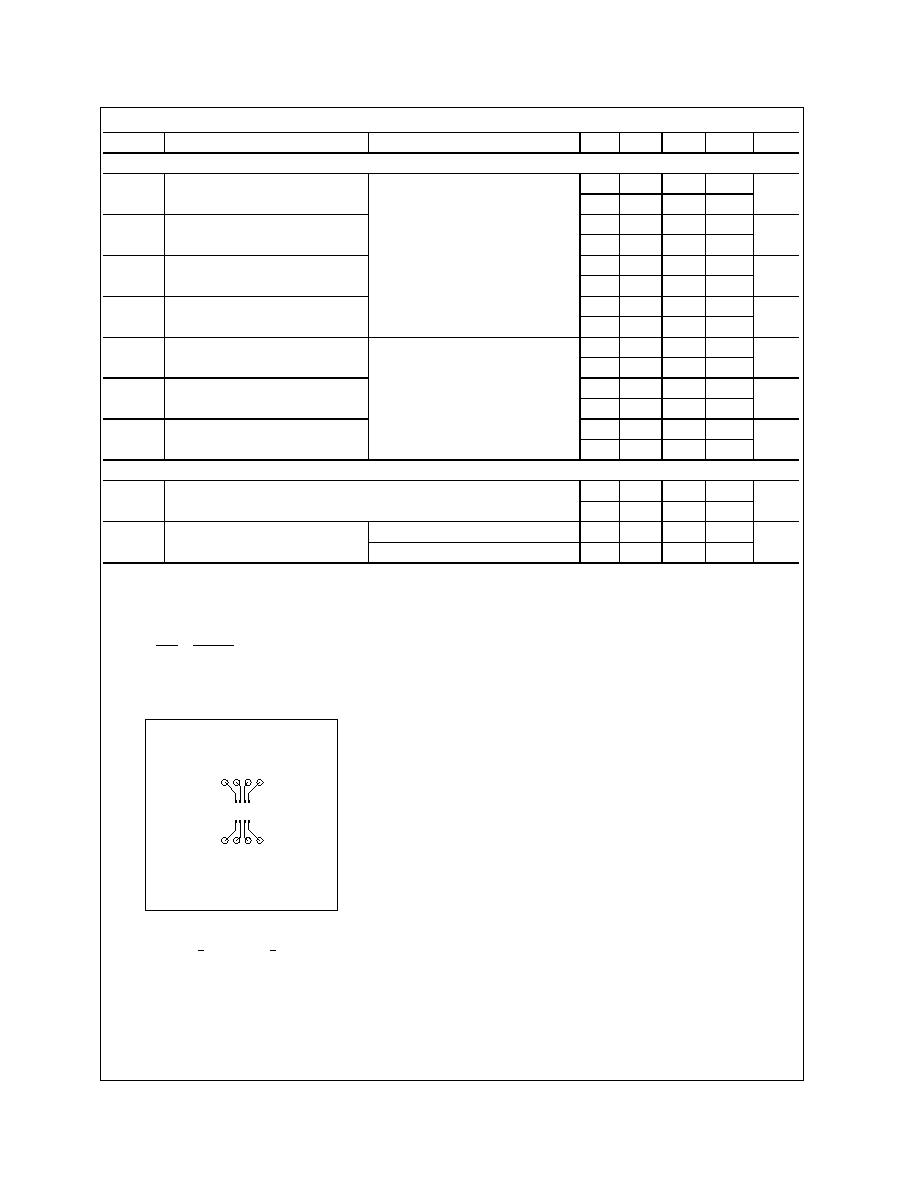
Electrical Characteristics
(T
A
= 25∞C unless otherwise noted)
Symbol
Parameter
Conditions
Type
Min
Typ
Max
Units
SWITCHING CHARACTERISTICS
(Note 2)
t
D(on)
Turn - On Delay Time
N-Channel
V
DD
= 5 V, I
D
= 1 A,
V
GEN
= 4.5 V, R
GEN
= 6
P-Channel
V
DD
= -5 V, I
D
= -1 A,
V
GEN
= -4.5 V, R
GEN
= 6
N-Ch
8
15
ns
P-Ch
10
20
t
r
Turn - On Rise Time
N-Ch
25
45
ns
P-Ch
27
50
t
D(off)
Turn - Off Delay Time
N-Ch
30
55
ns
P-Ch
37
65
t
f
Turn - Off Fall Time
N-Ch
8
15
ns
P-Ch
39
75
Q
g
Total Gate Charge
N-Channel
V
DS
= 10 V,
I
D
= 3 A, V
GS
= 4.5 V
P-Channel
V
DS
= -10 V,
I
D
= -2 A, V
GS
= -4.5 V
N-Ch
10
15
nC
P-Ch
7.8
11
Q
gs
Gate-Source Charge
N-Ch
0.9
nC
P-Ch
1.2
Q
gd
Gate-Drain Charge
N-Ch
3.5
nC
P-Ch
1.8
DRAIN-SOURCE DIODE CHARACTERISTICS AND MAXIMUM RATINGS
I
S
Maximum Continuous Drain-Source Diode Forward Current
N-Ch
0.67
A
P-Ch
-0.67
V
SD
Drain-Source Diode Forward Voltage
V
GS
= 0 V, I
S
= 0.67 A
(Note2)
N-Ch
0.7
1.2
V
V
GS
= 0 V, I
S
= -0.67 A
(Note2)
P-Ch
-0.75
-1.2
Notes:
1. R
JA
is the sum of the junction-to-case and case-to-ambient thermal resistance where the case thermal reference is defined as the solder mounting surface of the drain pins. R
JC
is guaranteed by
design while R
CA
is determined by the user's board design.
Typical R
JA
for single device operation using the board layout shown below on 4.5"x5" FR-4 PCB in a still air environment:
156
o
C/W when mounted on a 0.0025 in
2
pad of 2oz copper.
Scale 1 : 1 on letter size paper.
2. Pulse Test: Pulse Width < 300µs, Duty Cycle < 2.0%.
NDH8320C Rev.B
P
D
(
t
) =
T
J
-
T
A
R
J A
(
t
)
=
T
J
-
T
A
R
J C
+
R
CA
(
t
)
=
I
D
2
(
t
) ◊
R
DS
(
ON
)
@T
J
NDH8320C Rev.B
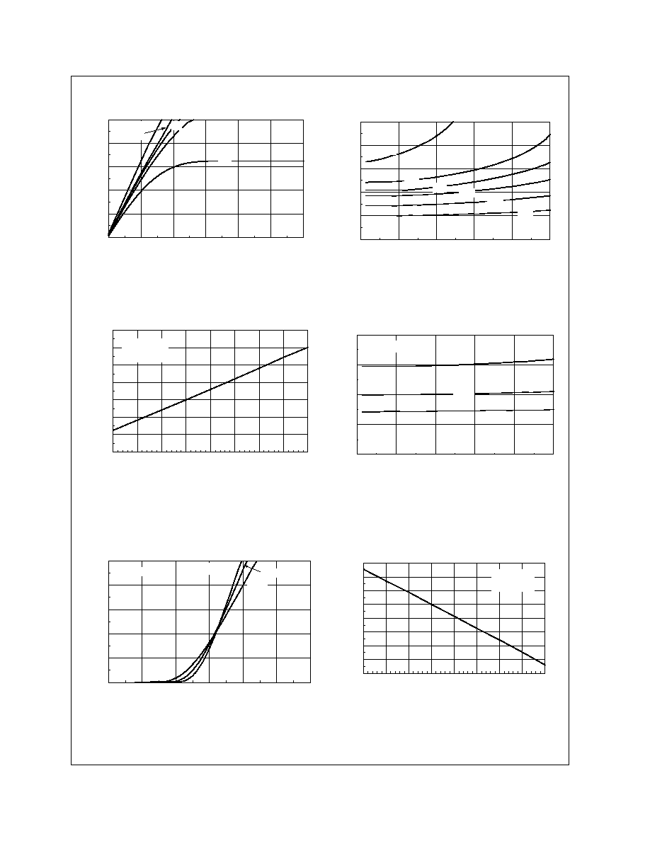
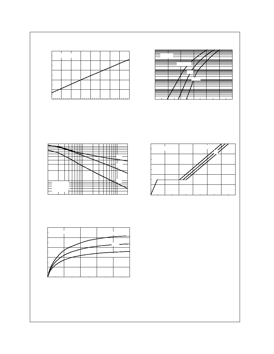
Typical Electrical Characteristics: N-Channel
Figure 1. N-Channel On-Region Characteristics.
Figure 2. N-Channel On-Resistance Variation with
Gate Voltage and Drain Current.
Figure 3. N-Channel On-Resistance Variation with
Temperature.
Figure 4. N-Channel On-Resistance Variation with Drain
Current and Temperature.
Figure 5. N-Channel Transfer
Characteristics.
Figure 6. N-Channel Gate Threshold Variation
with Temperature.
0
0.5
1
1.5
2
2.5
3
0
3
6
9
12
15
V , DRAIN-SOURCE VOLTAGE (V)
I , DRAIN-SOURCE CURRENT (A)
V =4.5V
GS
DS
D
2.0
2.7
3.0
2.5
0
3
6
9
12
15
0.75
1
1.25
1.5
1.75
2
I , DRAIN CURRENT (A)
DRAIN-SOURCE ON-RESISTANCE
V = 2.0V
GS
D
R , NORMALIZED
DS(on)
3.5
2.7
3.0
2.5
4.5
-50
-25
0
2 5
5 0
7 5
1 0 0
1 2 5
1 5 0
0 .4
0 .6
0 .8
1
1 .2
1 .4
1 .6
1 .8
T , JUNCTION TEMPERATURE (∞C)
DRAIN-SOURCE ON-RESISTANCE
J
R , NORMALIZED
DS(ON)
V = 4.5V
GS
I = 3A
D
0
3
6
9
12
15
0
0.5
1
1.5
2
I , DRAIN CURRENT (A)
DRAIN-SOURCE ON-RESISTANCE
V = 4.5V
GS
T = 125∞C
J
25∞C
-55∞C
D
R , NORMALIZED
DS(on)
0
0.5
1
1.5
2
2.5
3
0
2
4
6
8
10
V , GATE TO SOURCE VOLTAGE (V)
I , DRAIN CURRENT (A)
25∞C
125∞C
V =- 5V
DS
GS
D
T = -55∞C
J
-50
-25
0
25
50
75
100
125
150
0.5
0.6
0.7
0.8
0.9
1
1.1
1.2
1.3
T , JUNCTION TEMPERATURE (∞C)
GATE-SOURCE THRESHOLD VOLTAGE
J
V , NORMALIZED
th
I = 250µA
D
V = V
GS
DS
NDH8320C Rev.B
Figure 7. N-Channel Breakdown Voltage
Variation with Temperature.
Figure 8. N-Channel Body Diode Forward Voltage
Variation with Current and Temperature
.
Figure 9. N-Channel Capacitance Characteristics.
Figure 10. N-Channel Gate Charge Characteristics.
Typical Electrical Characteristics: N-Channel
(continued)
Figure 11. N-Channel Transconductance Variation
with Drain Current and Temperature.
-50
-25
0
25
50
75
100
125
150
0.9
0.95
1
1.05
1.1
1.15
T , JUNCTION TEMPERATURE (∞C)
DRAIN-SOURCE BREAKDOWN VOLTAGE
BV , NORMALIZED
DSS
J
I = 250µA
D
0
0.2
0.4
0.6
0.8
1
1.2
0.0001
0.001
0.01
0.1
1
5
10
V , BODY DIODE FORWARD VOLTAGE (V)
I , REVERSE DRAIN CURRENT (A)
T = 125∞C
J
25∞C
-55∞C
V =0V
GS
SD
S
0
2
4
6
8
1 0
1 2
0
1
2
3
4
5
Q , GATE CHARGE (nC)
V , GATE-SOURCE VOLTAGE (V)
g
GS
I = 3A
D
V = 5V
DS
10
15V
0 .1
0 .2
0 .5
1
3
5
1 0
2 0
4 0
1 0 0
2 0 0
3 0 0
5 0 0
8 0 0
1 2 0 0
V , DRAIN TO SOURCE VOLTAGE (V)
CAPACITANCE (pF)
DS
f = 1 MHz
V = 0 V
GS
C
oss
C
iss
C
rss
0
2
4
6
8
10
0
4
8
12
16
20
I , DRAIN CURRENT (A)
g , TRANSCONDUCTANCE (SIEMENS)
T = -55∞C
J
D
FS
V = 5V
DS
125∞C
25∞C