 | –≠–ª–µ–∫—Ç—Ä–æ–Ω–Ω—ã–π –∫–æ–º–ø–æ–Ω–µ–Ω—Ç: NDS9959 | –°–∫–∞—á–∞—Ç—å:  PDF PDF  ZIP ZIP |
February 1996
NDS9959
Dual N-Channel Enhancement Mode Field Effect Transistor
General Description
Features
_________________________________________________________________________________
Absolute Maximum Ratings
T
A
= 25∞C unless otherwise noted
Symbol
Parameter
NDS9959
Units
V
DSS
Drain-Source Voltage
50
V
V
GSS
Gate-Source Voltage
± 20
V
I
D
Drain Current - Continuous @ T
A
= 25∞C
(Note 1a)
± 2.0
A
- Continuous @ T
A
= 70∞C
(Note 1a)
± 1.6
- Pulsed @ T
A
= 25∞C
± 8
P
D
Power Dissipation for Dual Operation
2
W
Power Dissipation for Single Operation
(Note 1a)
1.6
(Note 1b)
1
(Note 1c)
0.9
T
J
,T
STG
Operating and Storage Temperature Range
-55 to 150
∞C
THERMAL CHARACTERISTICS
R
JA
Thermal Resistance, Junction-to-Ambient
(Note 1a)
78
∞C/W
R
JC
Thermal Resistance, Junction-to-Case
(Note 1)
40
∞C/W
NDS9959.SAM
These N-Channel enhancement mode power field effect
transistors are produced using Fairchild's proprietary, high cell
density, DMOS technology. This very high density process is
especially tailored to minimize on-state resistance, provide
superior switching performance, and withstand high energy
pulses in the avalanche and commutation modes. These
devices are particularly suited for low voltage applications such
as DC motor control and DC/DC conversion where fast
switching, low in-line power loss, and resistance to transients
are needed.
2.0A, 50V. R
DS(ON)
= 0.3
@ V
GS
= 10V
High density cell design for extremely low R
DS(ON)
.
High power and current handling capability in a widely used
surface mount package.
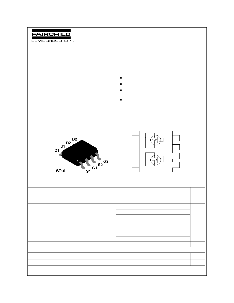
Dual MOSFET in surface mount package.
1
5
6
7
8
4
3
2
© 1997 Fairchild Semiconductor Corporation
Electrical Characteristics
(T
A
= 25∞C unless otherwise noted)
Symbol
Parameter
Conditions
Min
Typ
Max
Units
OFF CHARACTERISTICS
BV
DSS
Drain-Source Breakdown Voltage
V
GS
= 0 V, I
D
= 250 µA
50
V
I
DSS
Zero Gate Voltage Drain Current
V
DS
= 40 V, V
GS
= 0 V
2
µA
T
J
= 55∞C
25
µA
I
GSSF
Gate - Body Leakage, Forward
V
GS
= 20 V, V
DS
= 0 V
100
nA
I
GSSR
Gate - Body Leakage, Reverse
V
GS
= -20 V, V
DS
= 0 V
-100
nA
ON CHARACTERISTICS
(Note2)
V
GS(th)
Gate Threshold Voltage
V
DS
= V
GS
, I
D
= 250 µA
2
3
4
V
R
DS(ON)
Static Drain-Source On-Resistance
V
GS
= 10 V, I
D
= 1.5 A
0.3
V
GS
= 5 V, I
D
= 0.6 A
0.5
I
D(on)
On-State Drain Current
V
GS
= 10 V, V
DS
= 5 V
8
A
g
FS
Forward Transconductance
V
DS
= 15 V, I
D
= 2.0 A
1
2.7
S
DYNAMIC CHARACTERISTICS
C
iss
Input Capacitance
V
DS
= 25 V, V
GS
= 0 V,
f = 1.0 MHz
152
250
pF
C
oss
Output Capacitance
50
85
pF
C
rss
Reverse Transfer Capacitance
12
25
pF
SWITCHING CHARACTERISTICS
(Note 2)
t
D(on)
Turn - On Delay Time
V
DD
= 30 V, I
D
= 0.6 A,
V
GS
= 10 V, R
L
= 50
,
R
GEN
= 6
4
40
ns
t
r
Turn - On Rise Time
8
70
ns
t
D(off)
Turn - Off Delay Time
9
100
ns
t
f
Turn - Off Fall Time
11
70
ns
Q
g
Total Gate Charge
V
DS
= 25 V,
I
D
= 1.3 A, V
GS
= 10 V
4.3
15
nC
Q
gs
Gate-Source Charge
1.1
nC
Q
gd
Gate-Drain Charge
1.5
nC
NDS9959.SAM
Electrical Characteristics
(T
A
= 25∞C unless otherwise noted)
Symbol
Parameter
Conditions
Min
Typ
Max
Units
DRAIN-SOURCE DIODE CHARACTERISTICS AND MAXIMUM RATINGS
I
S
Maximum Continuos Drain-Source Diode Forward Current
1.8
A
V
SD
Drain-Source Diode Forward Voltage
V
GS
= 0 V, I
S
= 1.25 A
(Note 2)
0.84
1.2
V
t
rr
Reverse Recovery Time
V
GS
= 0V, I
F
= 1.25 A, dI
F
/dt = 100 A/µs
100
ns
Notes:
1. R
JA
is the sum of the junction-to-case and case-to-ambient thermal resistance where the case thermal reference is defined as the solder mounting surface of the drain pins. R
JC
is guaranteed by
design while R
CA
is determined by the user's board design.
P
D
(
t
) =
T
J
-
T
A
R
J A
(
t
)
=
T
J
-
T
A
R
J C
+
R
CA
(
t
)
=
I
D
2
(
t
) ◊
R
DS
(
ON
)
T
J
Typical R
JA
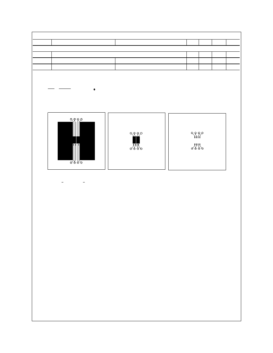
for single device operation using the board layouts shown below on 4.5"x5" FR-4 PCB in a still air environment:
a. 78
o
C/W when mounted on a 0.5 in
2
pad of 2oz cpper.
b. 125
o
C/W when mounted on a 0.02 in
2
pad of 2oz cpper.
c. 135
o
C/W when mounted on a 0.003 in
2
pad of 2oz cpper.
Scale 1 : 1 on letter size paper
2. Pulse Test: Pulse Width < 300µs, Duty Cycle < 2.0%.
NDS9959.SAM
1a
1b
1c
NDS9959.SAM
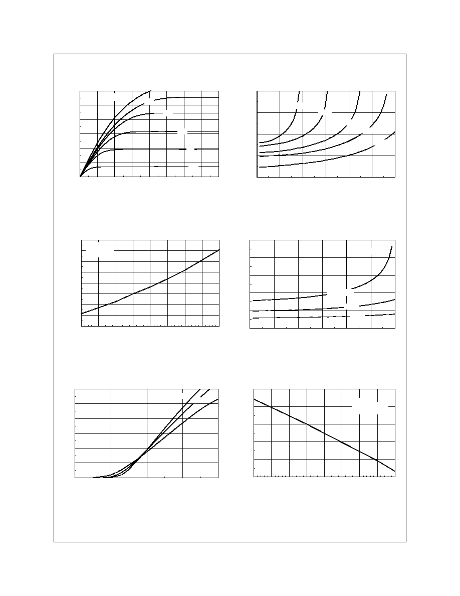
0
1
2
3
4
5
6
7
8
0
2
4
6
8
10
12
V , DRAIN-SOURCE VOLTAGE (V)
I , DRAIN-SOURCE CURRENT (A)
6.0
5.0
8.0
7.0
V =10V
DS
D
9.0
GS
-50
-25
0
25
50
75
100
125
150
0.4
0.6
0.8
1
1.2
1.4
1.6
1.8
2
T , JUNCTION TEMPERATURE (∞C)
DRAIN-SOURCE ON-RESISTANCE (OHMS)
J
V =10V
G S
I = 1.5A
D
R , NORMALIZED
DS(ON)
-50
-25
0
25
50
75
1 0 0
1 2 5
1 5 0
0.7
0.8
0.9
1
1.1
1.2
T , JUNCTION TEMPERATURE (∞C)
GATE-SOURCE THRESHOLD VOLTAGE (V)
J
I = 250µA
D
V = V
DS
GS
V , NORMALIZED
th
0
2
4
6
8
10
12
0.8
1.2
1.6
2
2.4
I , DRAIN CURRENT (A)
DRAIN-SOURCE ON-RESISTANCE
V = 6V
GS
D
R , NORMALIZED
DS(ON)
9.0V
10V
7.0V
8.0V
0
2
4
6
8
10
12
0
1
2
3
4
5
I , DRAIN CURRENT (A)
DRAIN-SOURCE ON-RESISTANCE
D
R , NORMALIZED
DS(ON)
V =10 V
GS
T = 125∞C
J
25∞C
-55∞C
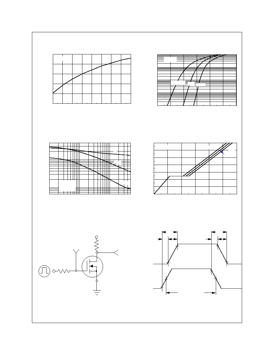
Typical Electrical Characteristics
Figure 1. On-Region Characteristics.
Figure 2. On-Resistance Variation with
Gate Voltage and Drain Current.
Figure 3. On-Resistance Variation
with Temperature.
Figure 4. On-Resistance Variation with Drain
Current and Temperature.
Figure 5. Transfer Characteristics.
Figure 6. Gate Threshold Variation with
Temperature.
2
4
6
8
1 0
0
2
4
6
8
1 0
1 2
V , GATE TO SOURCE VOLTAGE (V)
I , DRAIN CURRENT (A)
25
1 2 5
V = 10V
DS
GS
D
T = -55∞C
J
NDS9959.SAM
-50
-25
0
25
50
75
100
125
150
0.85
0.9
0.95
1
1.05
1.1
T , JUNCTION TEMPERATURE (∞C)
DRAIN-SOURCE BREAKDOWN VOLTAGE (V)
I = 250µA
D
BV , NORMALIZED
DSS
J
0.2
0.4
0.6
0.8
1
1.2
1.4
0.001
0.003
0.01
0.03
0.1
0.3
1
3
10
V , BODY DIODE FORWARD VOLTAGE (V)
I , REVERSE DRAIN CURRENT (A)
T = 125∞C
J
25∞C -55∞C
V =0V
GS
SD
S
0
1
2
3
4
5
6
0
2
4
6
8
10
12
14
Q , GATE CHARGE (nC)
V , GATE-SOURCE VOLTAGE (V)
g
GS
I = 1.3A
D
V = 10V
DS
20V
40V
0.1
0.2
0.5
1
2
5
10
20
50
10
20
50
100
200
400
V , DRAIN TO SOURCE VOLTAGE (V)
CAPACITANCE (pF)
DS
C iss
f = 1 MHz
V = 0V
GS
C oss
C
rss
G
D
S
V
DD
R
L
V
V
IN
OUT
V
GS
DUT
R
GEN
10%
50%
90%
10%
90%
90%
50%
V
IN
V
OUT
on
off
d(off)
f
r
d(on)
t
t
t
t
t
t
INVERTED
10%
PULSE WIDTH
Figure 7. Breakdown Voltage Variation with
Temperature.
Figure 8. Body Diode Forward Voltage
Variation with Current and Temperature
Figure 9. Capacitance Characteristics.
Figure 10. Gate Charge Characteristics.
Figure 11. Switching Test Circuit
Figure 12. Switching Waveforms
Typical Electrical Characteristics
(continued)