 | ÐлекÑÑоннÑй компоненÑ: NM24C03 | СкаÑаÑÑ:  PDF PDF  ZIP ZIP |
Äîêóìåíòàöèÿ è îïèñàíèÿ www.docs.chipfind.ru
1
www.fairchildsemi.com
NM24C02/03 Rev. G
NM24C02/03 2K-Bit Standard 2-Wire Bus Interface Serial EEPROM
February 2000
© 1998 Fairchild Semiconductor Corporation
NM24C02/03 2K-Bit Standard 2-Wire Bus
Interface Serial EEPROM
General Description
The NM24C02/03 devices are 2048 bits of CMOS non-volatile
electrically erasable memory. These devices conform to all speci-
fications in the Standard IIC 2-wire protocol and are designed to
minimize device pin count, and simplify PC board layout require-
ments.
The upper half (upper 1Kbit) of the memory of the NM24C03 can be
write protected by connecting the WP pin to V
CC
. This section of
memory then becomes unalterable unless WP is switched to V
SS
.
This communications protocol uses CLOCK (SCL) and DATA
I/O (SDA) lines to synchronously clock data between the master
(for example a microprocessor) and the slave EEPROM device(s).
The Standard IIC protocol allows for a maximum of 16K of
EEPROM memory which is supported by the Fairchild family in
2K, 4K, 8K, and 16K devices, allowing the user to configure the
memory as the application requires with any combination of
EEPROMs. In order to implement higher EEPROM memory
densities on the IIC bus, the Extended IIC protocol must be used.
(Refer to the NM24C32 or NM24C65 datasheets for more infor-
mation.)
Fairchild EEPROMs are designed and tested for applications requir-
ing high endurance, high reliability and low power consumption.
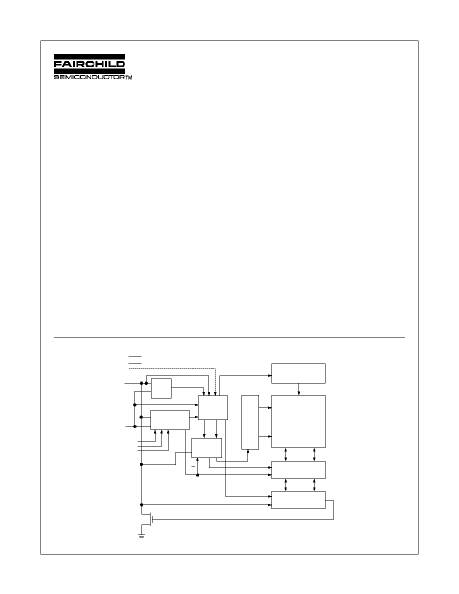
Block Diagram
Features
I Extended operating voltage 2.7V 5.5V
I 400 KHz clock frequency (F) at 2.7V - 5.5V
I 200µA active current typical
10
µA standby current typical
1
µA standby current typical (L)
0.1
µA standby current typical (LZ)
I IIC compatible interface
Provides bi-directional data transfer protocol
I Schmitt trigger inputs
I Sixteen byte page write mode
Minimizes total write time per byte
I Self timed write cycle
Typical write cycle time of 6ms
I Hardware Write Protect for upper half (NM24C03 only)
I Endurance: 1,000,000 data changes
I Data retention greater than 40 years
I Packages available: 8-pin DIP, 8-pin SO, and 8-pin TSSOP
I Available in three temperature ranges
- Commercial: 0
° to +70°C
- Extended (E): -40
° to +85C
- Automotive (V): -40
° to +125°C
H.V. GENERATION
TIMING &CONTROL
E2PROM
ARRAY
YDEC
DATA REGISTER
XDEC
CONTROL
LOGIC
WORD
ADDRESS
COUNTER
SLAVE ADDRESS
REGISTER &
COMPARATOR
START
STOP
LOGIC
CK
DIN
R/W
SDA
SCL
VSS
WP
VCC
DOUT
A2
A1
A0
DS500069-1
2
www.fairchildsemi.com
NM24C02/03 Rev. G
NM24C02/03 2K-Bit Standard 2-Wire Bus Interface Serial EEPROM
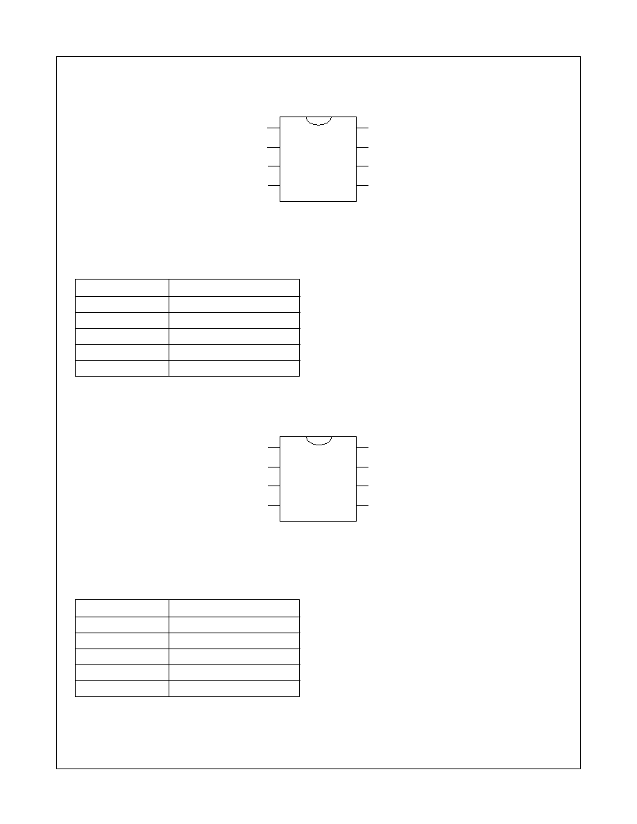
A0
A1
A2
VSS
VCC
NC
SCL
SDA
8
7
6
5
1
2
3
4
NM24C02
Connection Diagrams
Dual-in-Line Package (N), SO Package (M8) and TSSOP Package (MT8)
See Package Number N08E, M08A and MTC08
Pin Names
A0,A1,A2
Device Address Inputs
V
SS
Ground
SDA
Serial Data I/O
SCL
Serial Clock Input
NC
No Connection
V
CC
Power Supply
Dual-in-Line Package (N), SO Package (M8) and TSSOP Package (MT8)
See Package Number N08E, M08A and MTC08
Pin Names
A0,A1,A2
Device Address Inputs
V
SS
Ground
SDA
Serial Data I/O
SCL
Serial Clock input
WP
Write Protect
V
CC
Power Supply
A0
A1
A2
VSS
VCC
WP
SCL
SDA
8
7
6
5
1
2
3
4
NM24C03
DS500069-2
DS500069-3
3
www.fairchildsemi.com
NM24C02/03 Rev. G
NM24C02/03 2K-Bit Standard 2-Wire Bus Interface Serial EEPROM
Ordering Information
NM
24
C
XX
F
LZ
E
XXX
Letter
Description
Package
N
8-pin DIP
M8
8-pin SOIC
MT8
8-pin TSSOP
Temp. Range
None
0 to 70
°C
V
-40 to +125
°C
E
-40 to +85
°C
Voltage Operating Range
Blank
4.5V to 5.5V
L
2.7V to 5.5V
LZ
2.7V to 5.5V and
<1
µA Standby Current
SCL Clock Frequency
Blank
100KHz
F
400KHz
Density
02
2K
03
2K with Write Protect
C
CMOS Technology
Interface
24
IIC
NM
Fairchild Non-Volatile
Memory
4
www.fairchildsemi.com
NM24C02/03 Rev. G
NM24C02/03 2K-Bit Standard 2-Wire Bus Interface Serial EEPROM
Product Specifications
Absolute Maximum Ratings
Ambient Storage Temperature
65
°C to +150°C
All Input or Output Voltages
with Respect to Ground
6.5V to 0.3V
Lead Temperature
(Soldering, 10 seconds)
+300
°C
ESD Rating
2000V min.
Operating Conditions
Ambient Operating Temperature
NM24C02/03
0
°C to +70°C
NM24C02E/03E
-40
°C to +85°C
NM24C02V/03V
-40
°C to +125°C
Positive Power Supply
NM24C02/03
4.5V to 5.5V
NM24C02L/03L
2.7V to 5.5V
NM24C02LZ/03LZ
2.7V to 5.5V
DC Electrical Characteristics (2.7V to 5.5V)
Symbol
Parameter
Test Conditions
Limits
Units
Min
Typ
Max
(Note 1)
I
CCA
Active Power Supply Current
f
SCL
= 400 KHz
0.2
1.0
mA
f
SCL
= 100 KHz
I
SB
Standby Current
V
IN
= GND
V
CC
= 2.7V - 5.5V
10
50
µA
or V
CC
V
CC
= 2.7V - 5.5V (L)
1
10
µA
V
CC
= 2.7V - 4.5V (LZ)
0.1
1
µA
I
LI
Input Leakage Current
V
IN
= GND to V
CC
0.1
1
µA
I
LO
Output Leakage Current
V
OUT
= GND to V
CC
0.1
1
µA
V
IL
Input Low Voltage
0.3
V
CC
x 0.3
V
V
IH
Input High Voltage
V
CC
x 0.7
V
CC
+ 0.5
V
V
OL
Output Low Voltage
I
OL
= 3 mA
0.4
V
Capacitance
T
A
= +25
°C, f = 100/400 KHz, V
CC
= 5V
(Note 2)
Symbol
Test
Conditions
Max
Units
C
I/O
Input/Output Capacitance (SDA)
V
I/O
= 0V
8
pF
C
IN
Input Capacitance (A0, A1, A2, SCL)
V
IN
= 0V
6
pF
Note 1: Typical values are T
A
= 25
°C and nominal supply voltage of 5V for 4.5V-5.5V operation and at 3V for 2.7V-4.5V operation.
Note 2: This parameter is periodically sampled and not 100% tested.
5
www.fairchildsemi.com
NM24C02/03 Rev. G
NM24C02/03 2K-Bit Standard 2-Wire Bus Interface Serial EEPROM
AC Test Conditions
Input Pulse Levels
V
CC
x 0.1 to V
CC
x 0.9
Input Rise and Fall Times
10 ns
Input & Output Timing Levels
V
CC
x 0.3 to V
CC
x 0.7
Output Load
1 TTL Gate and C
L
= 100 pF
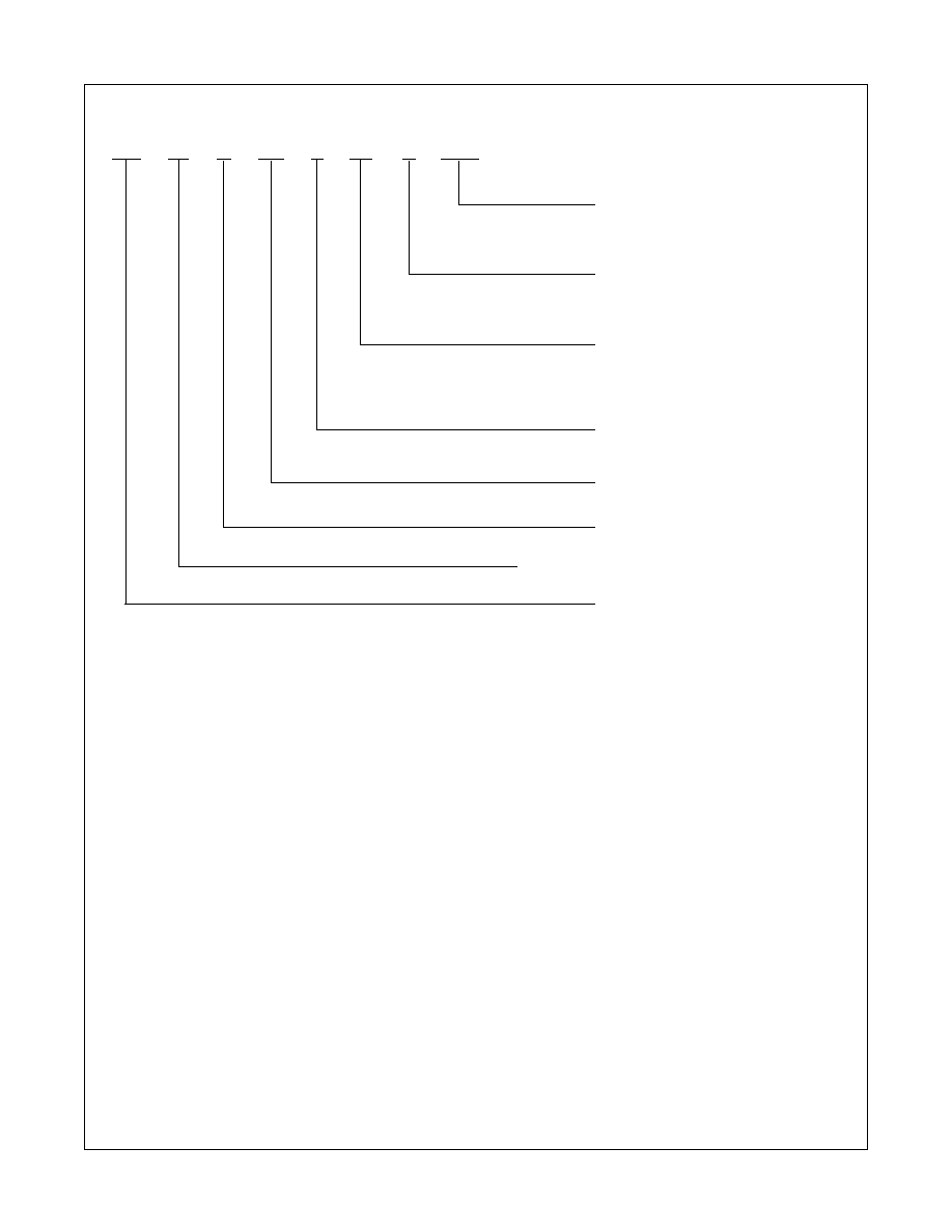
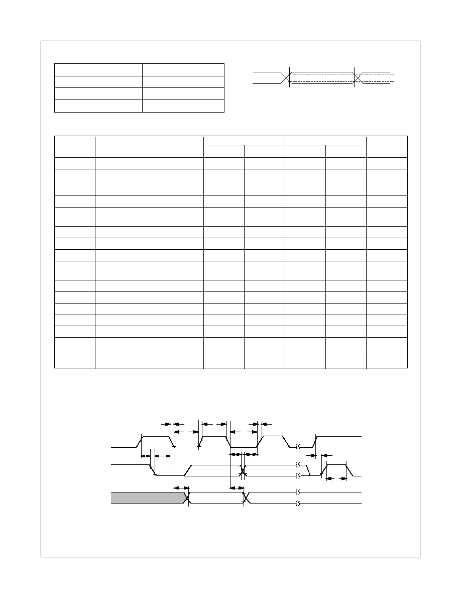
Bus Timing
DS500069-5
;;
SCL
SDA
IN
SDA
OUT
tF
tLOW
tHIGH
tR
tLOW
tAA
tDH
tBUF
tSU:STA
tHD:DAT
tHD:STA
tSU:DAT
tSU:STO
0.9V
CC
0.1V
CC
0.7V
CC
0.3V
CC
Read and Write Cycle Limits (Standard and Low V
CC
Range 2.7V - 5.5V)
Symbol
Parameter
100 KHz
400 KHz
Units
Min
Max
Min
Max
f
SCL
SCL Clock Frequency
100
400
KHz
T
I
Noise Suppression Time Constant at
SCL, SDA Inputs (Minimum V
IN
100
50
ns
Pulse width)
t
AA
SCL Low to SDA Data Out Valid
0.3
3.5
0.1
0.9
µs
t
BUF
Time the Bus Must Be Free before
4.7
1.3
µs
a New Transmission Can Start
t
HD:STA
Start Condition Hold Time
4.0
0.6
µs
t
LOW
Clock Low Period
4.7
1.5
µs
t
HIGH
Clock High Period
4.0
0.6
µs
t
SU:STA
Start Condition Setup Time
4.7
0.6
µs
(for a Repeated Start Condition)
t
HD:DAT
Data in Hold Time
20
20
ns
t
SU:DAT
Data in Setup Time
250
100
ns
t
R
SDA and SCL Rise Time
1
0.3
µs
t
F
SDA and SCL Fall Time
300
300
ns
t
SU:STO
Stop Condition Setup Time
4.7
0.6
µs
t
DH
Data Out Hold Time
300
50
ns
t
WR
Write Cycle Time - NM24C02/03
10
10
ms
(Note 3)
- NM24C02/03L, NM24C02/03LZ
15
15
Note 3: The write cycle time (t
WR
) is the time from a valid stop condition of a write sequence to the end of the internal erase/program cycle. During the write cycle, the
NM24C02/03 bus interface circuits are disabled, SDA is allowed to remain high per the bus-level pull-up resistor, and the device does not respond to its slave address. Refer
"Write Cycle Timing" diagram.
AC Testing Input/Output Waveforms
DS500069-4